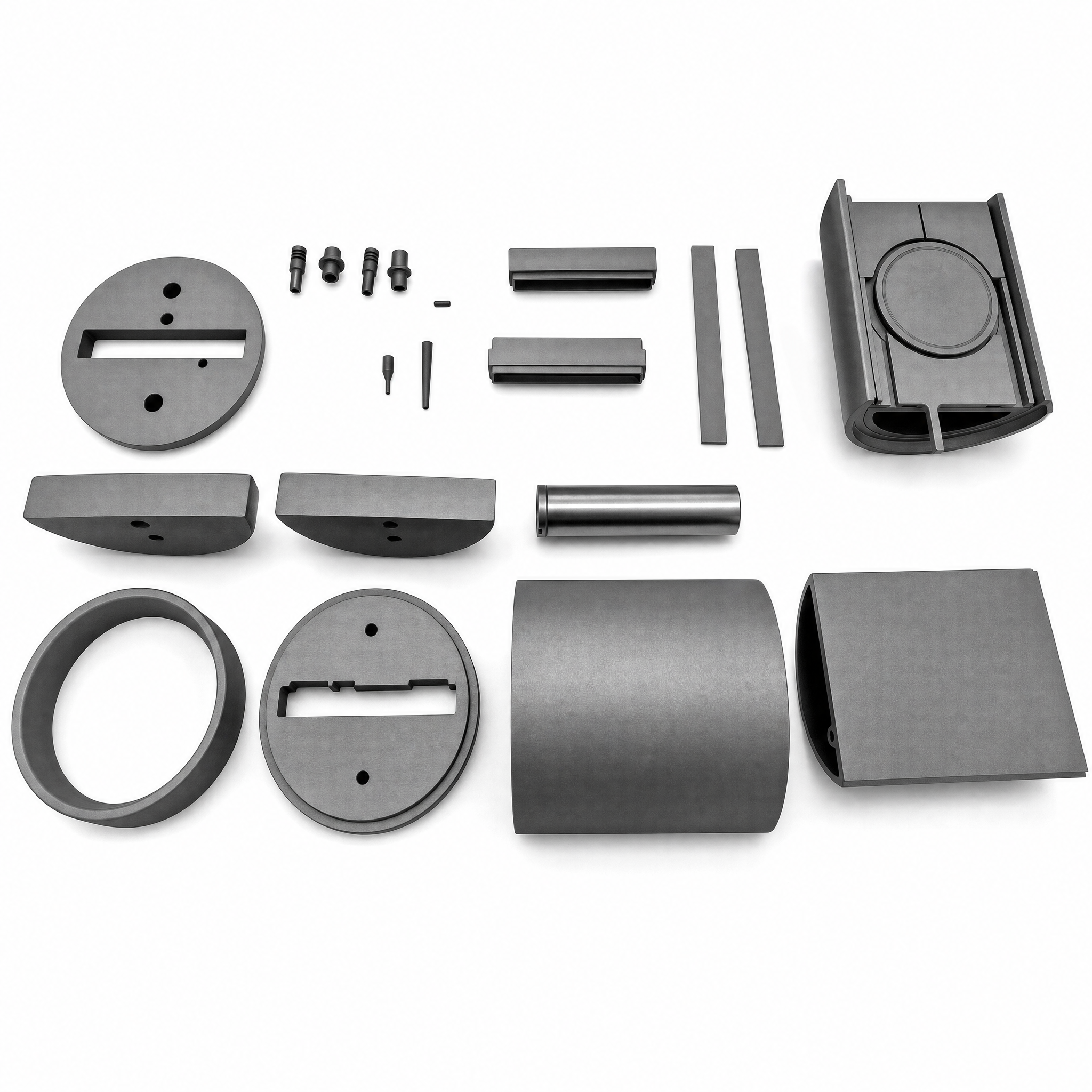
In the world of Silicon Carbide (SiC) semiconductors, most of the spotlight shines on 8-inch epitaxial reactors or the intricacies of wafer polishing. However, if we trace the supply chain back to the very beginning—inside the Physical Vapor Transport (PVT) furnace—a fundamental "material revolution" is quietly taking place.
In the era of rapid MEMS (Micro-Electromechanical Systems) evolution, selecting the right piezoelectric material is a make-or-break decision for device performance. PZT (Lead Zirconate Titanate) thin-film wafers have emerged as the premier choice over alternatives like AlN (Aluminum Nitride), offering superior electromechanical coupling for cutting-edge sensors and actuators.
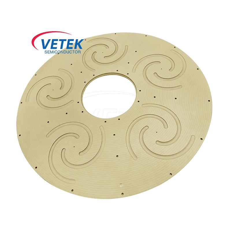
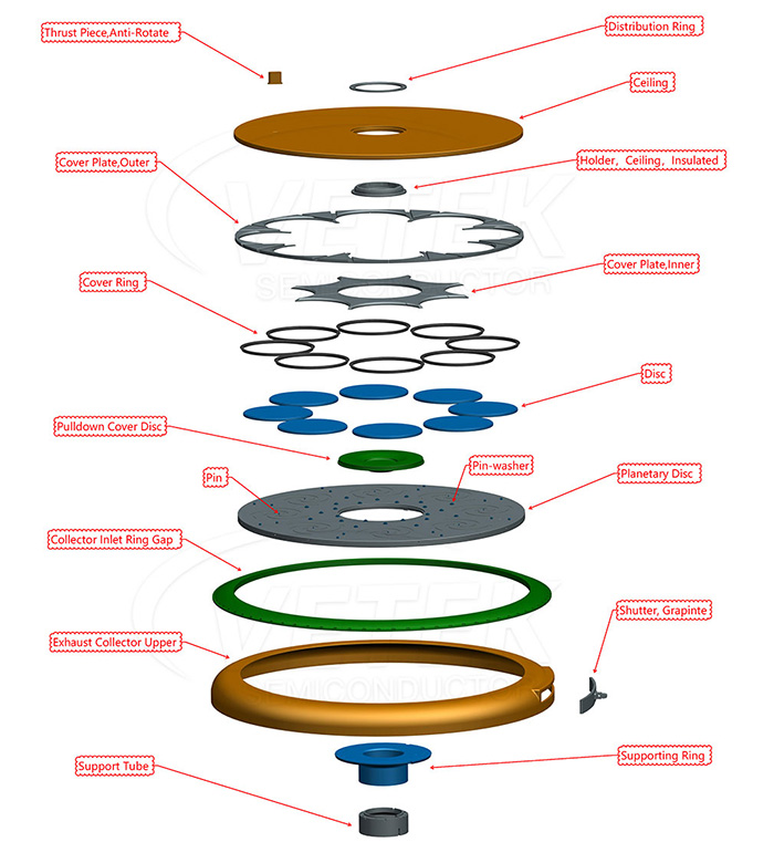
As semiconductor manufacturing continues to evolve toward advanced process nodes, higher integration, and complex architectures, the decisive factors for wafer yield are undergoing a subtle shift. For customized semiconductor wafer manufacturing, the breakthrough point for yield no longer lies solely in core processes like lithography or etching; high-purity susceptors are increasingly becoming the underlying variable affecting process stability and consistency.
We use cookies to offer you a better browsing experience, analyze site traffic and personalize content. By using this site, you agree to our use of cookies.Privacy Policy