
Products

China Silicon carbide E-Chuck Manufacturer, Supplier, Factory

We are going to dedicate ourselves to providing our esteemed buyers together with the most enthusiastically thoughtful products and services for Silicon carbide E-Chuck, GaN wafer etching process, Gallium nitride (GaN), Plasma etching (ICP/RIE) process, Etching process, We now have substantial goods source and also the rate is our advantage. Welcome to inquire about our merchandise.
Silicon carbide E-Chuck, we are sincerely hope to establish one good long term business relationship with your esteemed company thought this opportunity, based on equal, mutual beneficial and win win business from now till the future.

Hot Products

  • Porous SiC Ceramic Chuck

    Porous SiC Ceramic Chuck

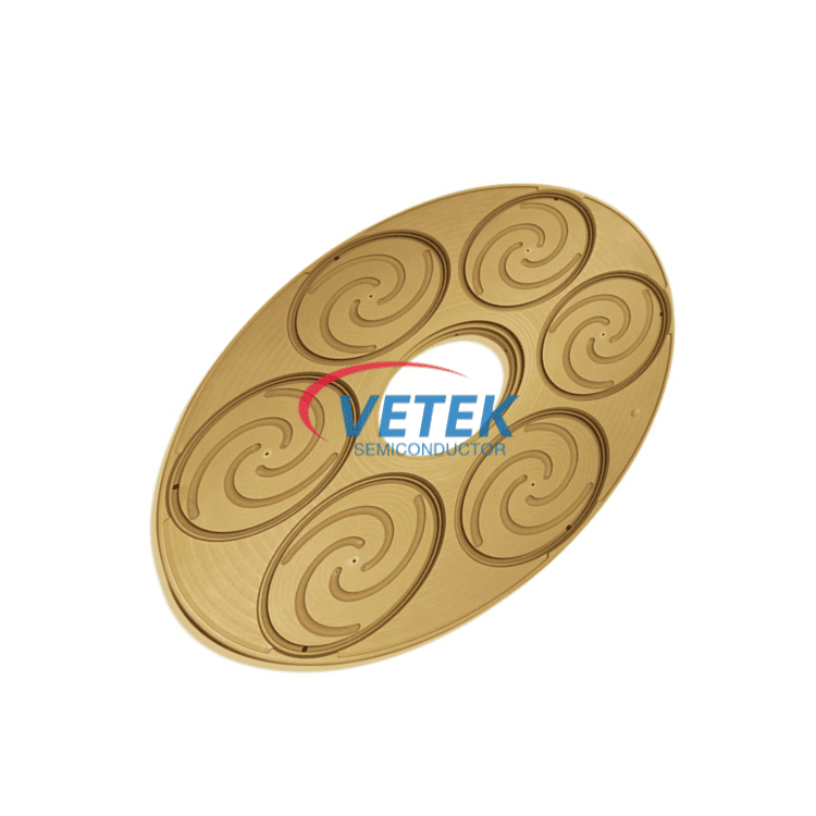
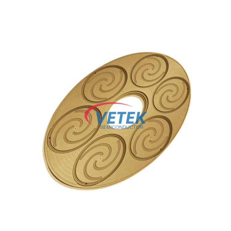
    Vetek Semiconductor offers Porous SiC Ceramic Chuck widely used in wafer processing technology, transfer and other links, suitable for bonding, scribing, patch, polishing and other links, laser processing. Our Porous SiC Ceramic Chuck has Ultra-strong vacuum adsorption, high flatness and high purity meet the needs of most semiconductor industries.Welcome to inquiry us.
  • SiC Ceramics Membrane

    SiC Ceramics Membrane

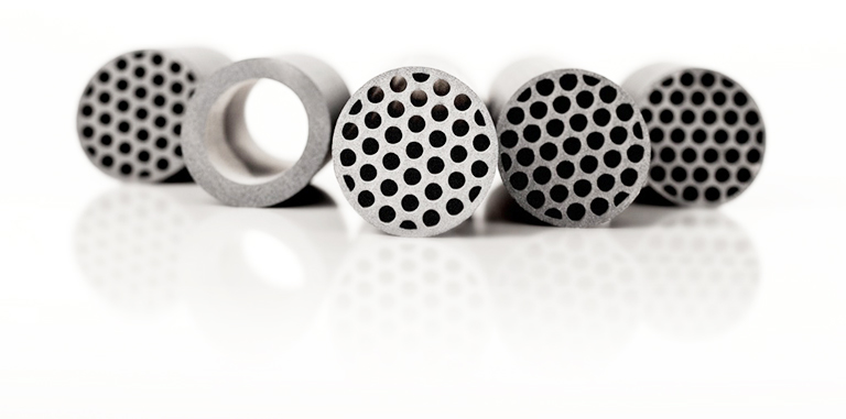
    Veteksemicon SiC ceramics membranes are a type of inorganic membrane and belong to solid membrane materials in membrane separation technology. SiC membranes are fired at a temperature above 2000℃. The surface of the particles is smooth and round. There are no closed pores or channels in the support layer and each layer. They are usually composed of three layers with different pore sizes.
  • Graphite Thermal Field

    Graphite Thermal Field

    At Vetek Semiconductor, graphite thermal fields are meticulously designed to meet the stringent standards of the photovoltaic industry, ensuring optimal performance and efficiency across various applications. We are dedicated to manufacturing high-performance graphite thermal fields that offer exceptional quality and cost-effectiveness.Pls no hesitate to contact us for any technical question or price.
  • Thermal spraying technology MLCC capacitor

    Thermal spraying technology MLCC capacitor

    Vetek Semiconductor thermal spraying technology plays an extremely important role in the coating application of sintered crucibles for high-end multilayer ceramic capacitor (MLCC) materials. With the continuous miniaturization and high performance of electronic devices, the demand for thermal spraying technology MLCC capacitors is also growing rapidly, especially in high-end applications. Looking forward to setting up long term business with you.
  • SiC Crystal Growth Porous Graphite

    SiC Crystal Growth Porous Graphite

    As a China leading SiC Crystal Growth Porous Graphite manufacturer , VeTek Semiconductor has been focusing on various Porous Graphite products for many years, such as Porous graphite crucible, High Purity Porous Graphite's investment and R&D, our Porous Graphite products have won high praise from European and American customers. Looking forward to your contact.
  • CVD SiC Coated Ceiling

    CVD SiC Coated Ceiling

    VeTek Semiconductor's CVD SiC coated ceiling has excellent properties such as high temperature resistance, corrosion resistance, high hardness, and low thermal expansion coefficient, making it an ideal material choice in semiconductor manufacturing. As a China leading CVD SiC coated ceiling manufacturer and supplier, VeTek semiconductor looks forward to your consultation.

Send Inquiry

X
We use cookies to offer you a better browsing experience, analyze site traffic and personalize content. By using this site, you agree to our use of cookies.Privacy Policy
RejectAccept