
Products

China GaN wafer etching process Manufacturer, Supplier, Factory

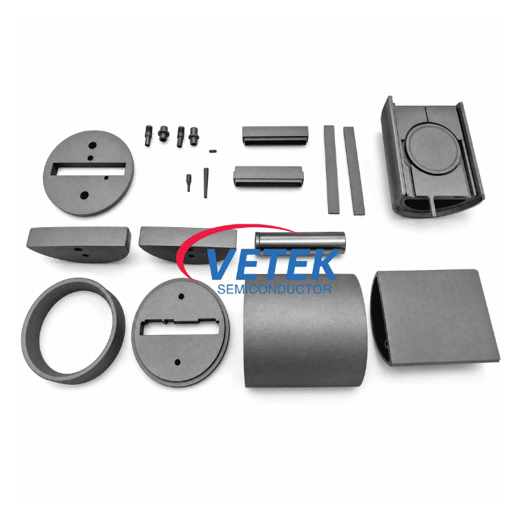
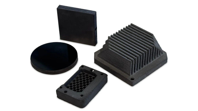
We usually keep on with the principle "Quality To start with, Prestige Supreme". We've been fully committed to offering our purchasers with competitively priced excellent solutions, prompt delivery and skilled support for GaN wafer etching process, Gallium nitride (GaN), Plasma etching (ICP/RIE) process, Etching process, SiC coated E-Chuck, We give priority to good quality and customer fulfillment and for this we follow stringent excellent control measures. We've in-house testing facilities where our goods are tested on each and every aspect at different processing stages. Owning to latest technologies, we facilitate our prospects with custom-made production facility.
GaN wafer etching process, Our products have mainly exported to south-east Asia Euro-America, and sales to all of our country. And depending on excellent quality, reasonable price, best service, we have got good feedback from customers overseas. You are welcomed to join us for more possibilities and benefits. We welcome customers, business associations and friends from all parts of the world to contact us and seek cooperation for mutual benefits.

Hot Products

  • Porous SiC Vacuum Chuck

    Porous SiC Vacuum Chuck

    Vetek Semiconductor's Porous SiC Vacuum Chuck is usually used in key components of semiconductor manufacturing equipment, especially when it comes to CVD and PECVD processes. Vetek Semiconductor specializes in manufacturing and supplying high-performance Porous SiC Vacuum Chuck. Welcome for your further inquiries.
  • TaC Coated ring

    TaC Coated ring

    As a leading manufacturer and supplier of TaC Coated ring products in China, VeTek Semiconductor has been focusing on the R&D and production of various TaC coating products. As the main customers of TaC Coating products, European and American manufacturers have given high praise to our coating products. Welcome to your further consultation.
  • SiC coated deep UV LED susceptor

    SiC coated deep UV LED susceptor

    SiC coated deep UV LED susceptor is designed for MOCVD process to support efficient and stable deep UV LED epitaxial layer growth. VeTek Semiconductor is a leading manufacturer and supplier of SiC coated deep UV LED susceptor in China. We have rich experience and have established long-term cooperative relationships with many LED epitaxial manufacturers.We are the top domestic manufacturer of susceptor products for LEDs. After years of verification, our product life span is on par with that of top international manufacturers. Looking forward to your inquiry.
  • Glassy Carbon Crucible

    Glassy Carbon Crucible

    As a leading Chinese manufacturer of Glassy Carbon products, Veteksemicon's Glassy Carbon Crucibles are widely used in the semiconductor manufacturing field due to their excellent ultra-high purity, zero porosity, anti-permeation and excellent chemical corrosion resistance, and have won high praise from European and American customers. Welcome to your inquiry.
  • Monocrystalline pulling Crucible

    Monocrystalline pulling Crucible

    Graphite crucible is an important part of Monocrystalline Pulling Crucibles in the process of achieving monocrystalline silicon ingot growth.Vetek semiconductor's crucibles are intricately engineered to meet the rigorous requirements set by the semiconductor industry.We are committed to producing and supplying crystal growth graphite crucibles that excel in performance, quality, and cost-effectiveness to meet the evolving needs of the industry.Welcome to inquiry us.
  • Large sized resistance heating SiC crystal growth furnace

    Large sized resistance heating SiC crystal growth furnace

    Silicon carbide crystal growth is a core process in the manufacturing of high-performance semiconductor devices. The stability, precision, and compatibility of crystal growth equipment directly determine the quality and yield of silicon carbide ingots. Based on the characteristics of Physical Vapor Transport (PVT) technology, Veteksemi has developed a resistance heating furnace for silicon carbide crystal growth, enabling stable growth of 6-inch, 8-inch, and 12-inch silicon carbide crystals with full compatibility with conductive, semi-insulating, and N-type material systems. Through precise control of temperature, pressure, and power, it effectively reduces crystal defects such as EPD (Etch Pit Density) and BPD (Basal Plane Dislocation), while featuring low energy consumption and a compact design to meet the high standards of industrial large-scale production.

Send Inquiry

X
We use cookies to offer you a better browsing experience, analyze site traffic and personalize content. By using this site, you agree to our use of cookies.Privacy Policy