
Products

China RTP RTA Carrier Manufacturer, Supplier, Factory

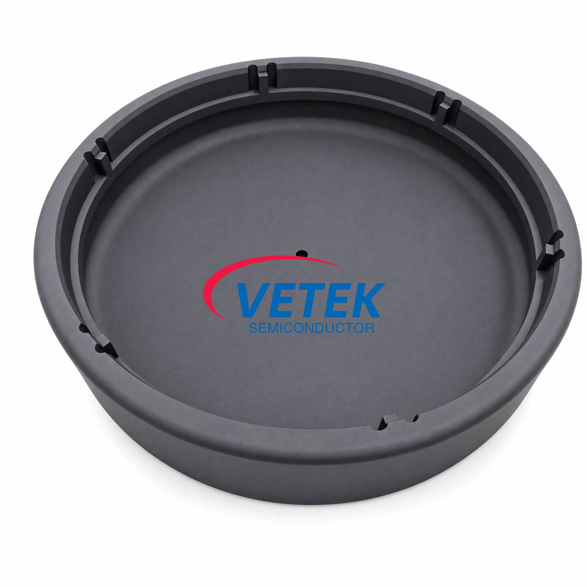
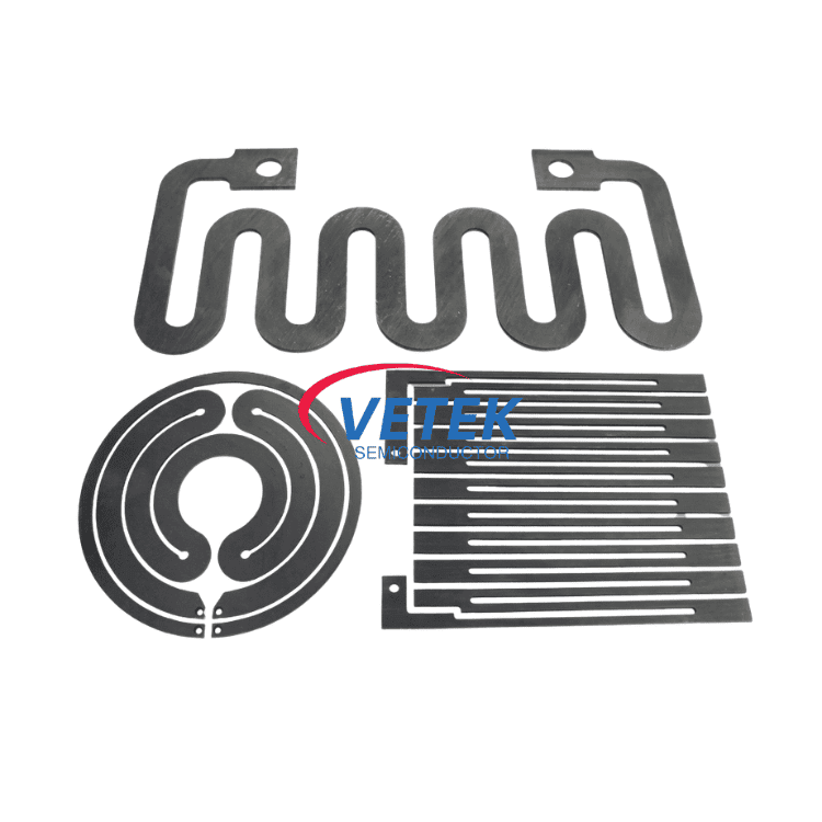
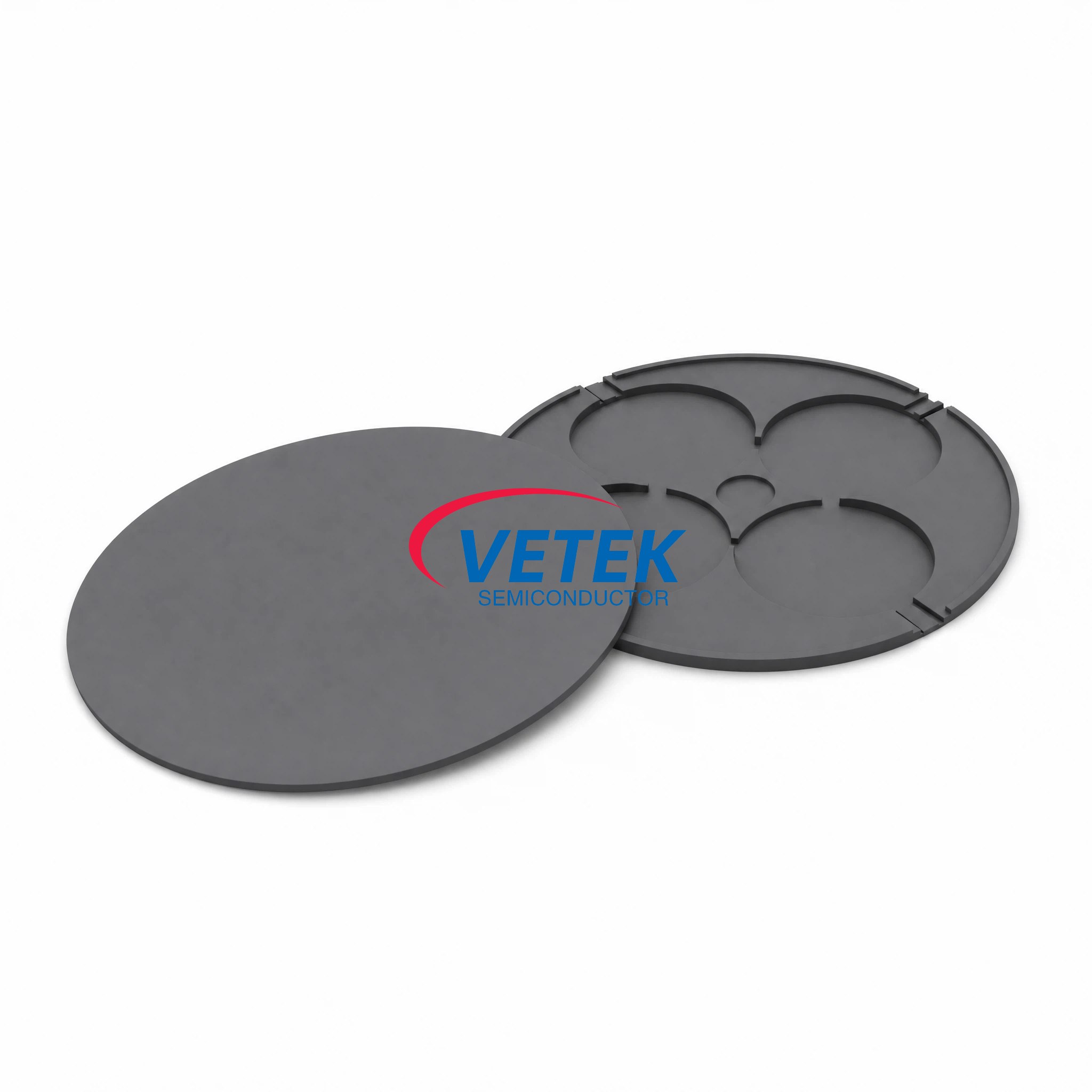
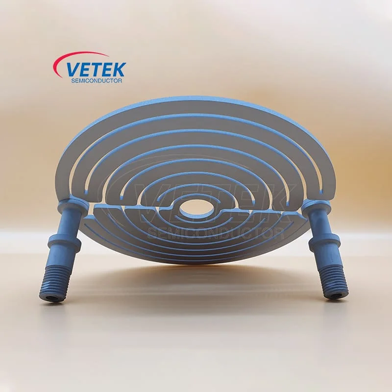
We know that we only thrive if we will guarantee our combined cost competiveness and high-quality advantageous at the same time for RTP RTA Carrier, CVD SiC Coated Graphite RTP RTA Carrier, SiC Coated RTP Carrier, Graphite RTP Carrier, Semiconductor RTP Carrier, We glance ahead to supplying you with our goods from the near long run, and you'll find our quotation is very acceptable plus the top quality of our goods is quite outstanding!
RTP RTA Carrier, Our business activities and processes are engineered to make sure our customers have access to widest range of products with the shortest supply time lines. This achievement is made possible by our highly skilled and experienced team. We look for people who want to grow with us around the globe and stand out from the crowd. We now have people who embrace tomorrow, have vision, love stretching their minds and going far beyond what they thought was achievable.
Hot Products

  • SiC Coated Barrel Susceptor for LPE PE2061S

    SiC Coated Barrel Susceptor for LPE PE2061S

    As one of the leading wafer susceptor manufacturing plants in China, VeTek Semiconductor has made continuous progress in wafer susceptor products and has become the first choice for many epitaxial wafer manufacturers. The SiC Coated Barrel Susceptor for LPE PE2061S provided by VeTek Semiconductor is designed for LPE PE2061S 4'' wafers. The susceptor has a durable silicon carbide coating that improves performance and durability during the LPE (liquid phase epitaxy) process. Welcome your inquiry, we look forward to becoming your long-term partner.
  • SiC Coating Cover Segments

    SiC Coating Cover Segments

    Vtech Semiconductor is committed to the development and commercialization of CVD SiC coated parts for Aixtron reactors. As an example, our SiC Coating Cover Segments have been carefully processed to produce a dense CVD SiC coating with excellent corrosion resistance, chemical stability, welcome to discuss application scenarios with us.
  • CVD SiC coating ring

    CVD SiC coating ring

    The CVD SiC coating ring is one of the important parts of the halfmoon parts. Together with other parts, it forms the SiC epitaxial growth reaction chamber. VeTek Semiconductor is a professional CVD SiC coating ring manufacturer and supplier. According to the customer's design requirements, we can provide the corresponding CVD SiC coating ring at the most competitive price. VeTek Semiconductor looks forward to becoming your long-term partner in China.
  • Crucible for Monocrystalline Silicon

    Crucible for Monocrystalline Silicon

    The thermal field of the monocrystal silicon furnace uses graphite as the crucible, and uses the heater, guide ring, bracket and pot holder made of isostatic pressed graphite to ensure the strength and purity of the graphite crucible. Vetek semiconductor produces crucible for Monocrystalline Silicon, long life, high purity, welcome to consult us.
  • Ion Beam Sputter sources grid

    Ion Beam Sputter sources grid

    Ion beam is mainly used for ion etching, ion coating and plasma injection. The role of the Ion Beam Sputter sources grid is to dissect the ions and accelerate them to the required energy. Vetek Semiconductor provides high purity graphite ion beam Ion Beam Sputter sources grid for optical lens ion beam polishing, semiconductor wafer modification, etc. Welcome to inquire about customized products.
  • Large sized resistance heating SiC crystal growth furnace

    Large sized resistance heating SiC crystal growth furnace

    Silicon carbide crystal growth is a core process in the manufacturing of high-performance semiconductor devices. The stability, precision, and compatibility of crystal growth equipment directly determine the quality and yield of silicon carbide ingots. Based on the characteristics of Physical Vapor Transport (PVT) technology, Veteksemi has developed a resistance heating furnace for silicon carbide crystal growth, enabling stable growth of 6-inch, 8-inch, and 12-inch silicon carbide crystals with full compatibility with conductive, semi-insulating, and N-type material systems. Through precise control of temperature, pressure, and power, it effectively reduces crystal defects such as EPD (Etch Pit Density) and BPD (Basal Plane Dislocation), while featuring low energy consumption and a compact design to meet the high standards of industrial large-scale production.

Send Inquiry

X
We use cookies to offer you a better browsing experience, analyze site traffic and personalize content. By using this site, you agree to our use of cookies.Privacy Policy