
Products

China Ion beam etching Manufacturer, Supplier, Factory

Our eternal pursuits are the attitude of "regard the market, regard the custom, regard the science" as well as the theory of "quality the basic, have confidence in the very first and management the advanced" for Ion beam etching, Vetek Semiconductor graphite material, Etching processes, High purity graphite, Etching techniques, Our goods are strictly inspected before exporting , So we gain a excellent standing all around the planet. We wanting ahead to cooperation with you in the foreseeable future.
Ion beam etching, We welcome an opportunity to do business with you and hope to have pleasure in attaching further details of our products and solutions. Excellent quality, competitive price, punctual delivery and dependable service can be guaranteed. For further inquires please do not hesitate to contact us.

Hot Products

  • Plasma Etching Focus Ring

    Plasma Etching Focus Ring

    An important component used in the wafer fabrication etching process is the plasma etching focus ring, whose function is to hold the wafer in place to maintain plasma density and prevent contamination of the wafer sides.Vetek semiconductor provide plasma etching focus ring with different material like monocrystalline silicon, silicon carbide, boron carbide and other ceramic materials.
  • CVD TaC Coating Cover

    CVD TaC Coating Cover

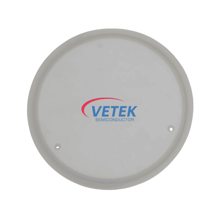
    CVD TaC coating cover provided by VeTek Semiconductor is a highly specialized component designed specifically for demanding applications. With its advanced features and exceptional performance, our CVD TaC coating cover offers several key advantages.Our CVD TaC coating cover provides the necessary protection and performance required for success.We looking forward to exploring potential cooperation with you!
  • Solid SiC Focus Ring

    Solid SiC Focus Ring

    Veteksemi solid SiC focus ring significantly improves etching uniformity and process stability by precisely controlling the electric field and airflow at the wafer edge. It is widely used in precision etching processes for silicon, dielectrics, and compound semiconductor materials, and is a key component for ensuring mass production yield and long-term reliable equipment operation.
  • Silicon Carbide Shower Head

    Silicon Carbide Shower Head

    Silicon Carbide Shower Head has excellent high temperature tolerance, chemical stability, thermal conductivity and good gas distribution performance, which can achieve uniform gas distribution and improve film quality. Therefore, it is usually used in high temperature processes such as chemical vapor deposition (CVD) or physical vapor deposition (PVD) processes. Welcome your further consultation to us ,vetek semiconductor.
  • Porous SiC Ceramic Chucks

    Porous SiC Ceramic Chucks

    The Porous SiC Ceramic Chuck by Veteksemicon is a precision-engineered vacuum platform designed for secure and particle-free wafer handling in advanced semiconductor processes such as etching, ion implantation, CMP, and inspection. Manufactured from high-purity porous silicon carbide, it offers outstanding thermal conductivity, chemical resistance, and mechanical strength. With customizable pore sizes and dimensions, Veteksemicon delivers tailored solutions to meet the stringent demands of cleanroom wafer processing environments.
  • Aixtron Satellite wafer carrier

    Aixtron Satellite wafer carrier

    VeTek Semiconductor’s Aixtron Satellite Wafer Carrier is a wafer carrier used in AIXTRON equipment, mainly used in MOCVD processes, and is particularly suitable for high-temperature and high-precision semiconductor processing processes. The carrier can provide stable wafer support and uniform film deposition during MOCVD epitaxial growth, which is essential for the layer deposition process. Welcome your further consultation.

Send Inquiry

X
We use cookies to offer you a better browsing experience, analyze site traffic and personalize content. By using this site, you agree to our use of cookies.Privacy Policy