Products

China Etching techniques Manufacturer, Supplier, Factory

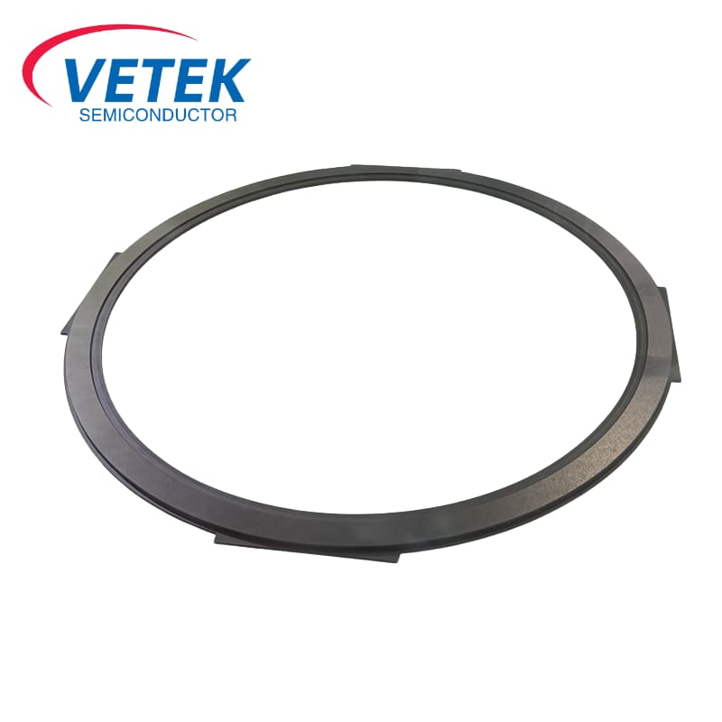
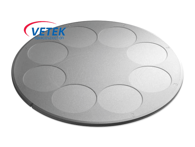
The very rich projects management experiences and one to one service model make the high importance of business communication and our easy understanding of your expectations for Etching techniques, Vetek Semiconductor graphite material, Etching processes, Ion beam etching, High purity graphite, Our tenet is evident each of the time: to provide good quality solution at competitive rate to clients throughout the planet. We welcome potential purchasers to call us for OEM and ODM orders.
Etching techniques, Now, we professionally supplies customers with our main products And our business is not only the "buy" and "sell", but also focus on more. We target to be your loyal supplier and long-term cooperator in China. Now, We hope to be the friends with you.

Hot Products

  • 4 Inch Insulation Rigid Felt - Body

    4 Inch Insulation Rigid Felt - Body

    4 Inch Insulation Rigid Felt - Body provided by VeTek Semiconductor is a rigid insulation material made of high-quality carbon fiber material. It has excellent insulation performance and durability. It can effectively insulate heat, sound and shock, and is suitable for a variety of applications. VeTek Semiconductor looks forward to establishing a long-term cooperative relationship with you and becoming a partner in the global market.Welcome to inquire.
  • SiC Crystal Growth Porous Graphite

    SiC Crystal Growth Porous Graphite

    As a China leading SiC Crystal Growth Porous Graphite manufacturer , VeTek Semiconductor has been focusing on various Porous Graphite products for many years, such as Porous graphite crucible, High Purity Porous Graphite's investment and R&D, our Porous Graphite products have won high praise from European and American customers. Looking forward to your contact.
  • Wafer Chuck

    Wafer Chuck

    Wafer chunk a wafer clamping tool in semiconductor process and is widely used in PVD, CVD, ETCH and other process.Vetek Semiconductor's wafer chuck play pivotal roles in semiconductor production, enabling fast, high-quality output. With in-house manufacturing, competitive pricing, and robust R&D support, Vetek Semiconductor excels in OEM/ODM services for precision components.Looking forward to your inquiry.
  • Hot Zone graphite heater

    Hot Zone graphite heater

    Veteksemicon Hot Zone graphite heater is designed to handle the extreme conditions in high temperature furnaces and maintain excellent performance and stability in complex processes such as chemical vapor deposition (CVD), epitaxial growth and high temperature annealing. Veteksemicon always focuses on producing and providing high-quality Hot Zone graphite heaters. We sincerely invite you to contact us.
  • Large sized resistance heating SiC crystal growth furnace

    Large sized resistance heating SiC crystal growth furnace

    Silicon carbide crystal growth is a core process in the manufacturing of high-performance semiconductor devices. The stability, precision, and compatibility of crystal growth equipment directly determine the quality and yield of silicon carbide ingots. Based on the characteristics of Physical Vapor Transport (PVT) technology, Veteksemi has developed a resistance heating furnace for silicon carbide crystal growth, enabling stable growth of 6-inch, 8-inch, and 12-inch silicon carbide crystals with full compatibility with conductive, semi-insulating, and N-type material systems. Through precise control of temperature, pressure, and power, it effectively reduces crystal defects such as EPD (Etch Pit Density) and BPD (Basal Plane Dislocation), while featuring low energy consumption and a compact design to meet the high standards of industrial large-scale production.
  • Silicon Carbide Seal Ring

    Silicon Carbide Seal Ring

    As a professional Silicon Carbide Seal Ring product manufacturer and factory in China, VeTek Semiconductor Silicon Carbide Seal Ring is widely used in semiconductor processing equipment due to its excellent heat resistance, corrosion resistance, mechanical strength and thermal conductivity. It is especially suitable for processes involving high temperature and reactive gases such as CVD, PVD and plasma etching, and is a key material choice in the semiconductor manufacturing process. Your further inquiries are welcome.

Send Inquiry

X
We use cookies to offer you a better browsing experience, analyze site traffic and personalize content. By using this site, you agree to our use of cookies. Privacy Policy
Reject Accept