
Products

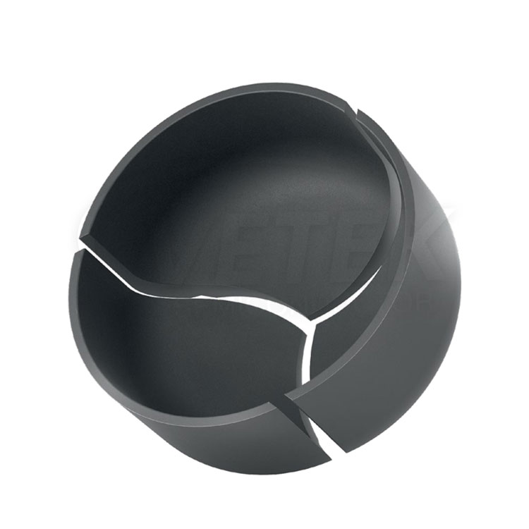
China Tantalum Carbide Coated Porous Graphite Manufacturer, Supplier, Factory

We believe in: Innovation is our soul and spirit. Quality is our life. Customer need is our God for Tantalum Carbide Coated Porous Graphite, Should additional details be required, please call us anytime!
Tantalum Carbide Coated Porous Graphite, We have been persisting in the business essence "Quality First, Honoring Contracts and Standing by Reputations, providing customers with satisfying merchandise and service. " Friends both at home and abroad are warmly welcome to establish everlasting business relations with us.
Hot Products

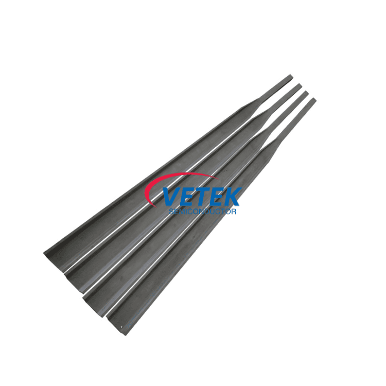
  • Silicon carbide Cantilever Paddle for Wafer Processing

    Silicon carbide Cantilever Paddle for Wafer Processing

    The Silicon Carbide Cantilever Paddle from Veteksemicon is engineered for advanced wafer processing in semiconductor manufacturing. Made of high-purity SiC, it delivers outstanding thermal stability, superior mechanical strength, and excellent resistance to high temperatures and corrosive environments. These features ensure precise wafer handling, extended service life, and reliable performance in processes such as MOCVD, epitaxy, and diffusion. Welcome to consult.
  • SiC Coated Support for LPE PE2061S

    SiC Coated Support for LPE PE2061S

    VeTek Semiconductor is a leading manufacturer and supplier of SiC Coated graphite components in China. SiC Coated Support for LPE PE2061S is suitable for LPE silicon epitaxial reactor. As the bottom of the barrel base, SiC Coated Support for LPE PE2061S can withstand high temperatures of 1600 degrees Celsius, thereby achieving ultra-long product life and reducing customer costs. Looking forward to your inquiry and further communication.
  • TaC Coating Heater

    TaC Coating Heater

    VeTek Semiconductor TaC Coating Heater has an extremely high melting point (about 3880°C). The high melting point enables it to operate at extremely high temperatures, especially in the growth of gallium nitride (GaN) epitaxial layers in the metal organic chemical vapor deposition (MOCVD) process. VeTek Semiconductor is committed to providing customers with customized product solutions. We look forward to hearing from you.
  • Quartz Gas Distribution Plate

    Quartz Gas Distribution Plate

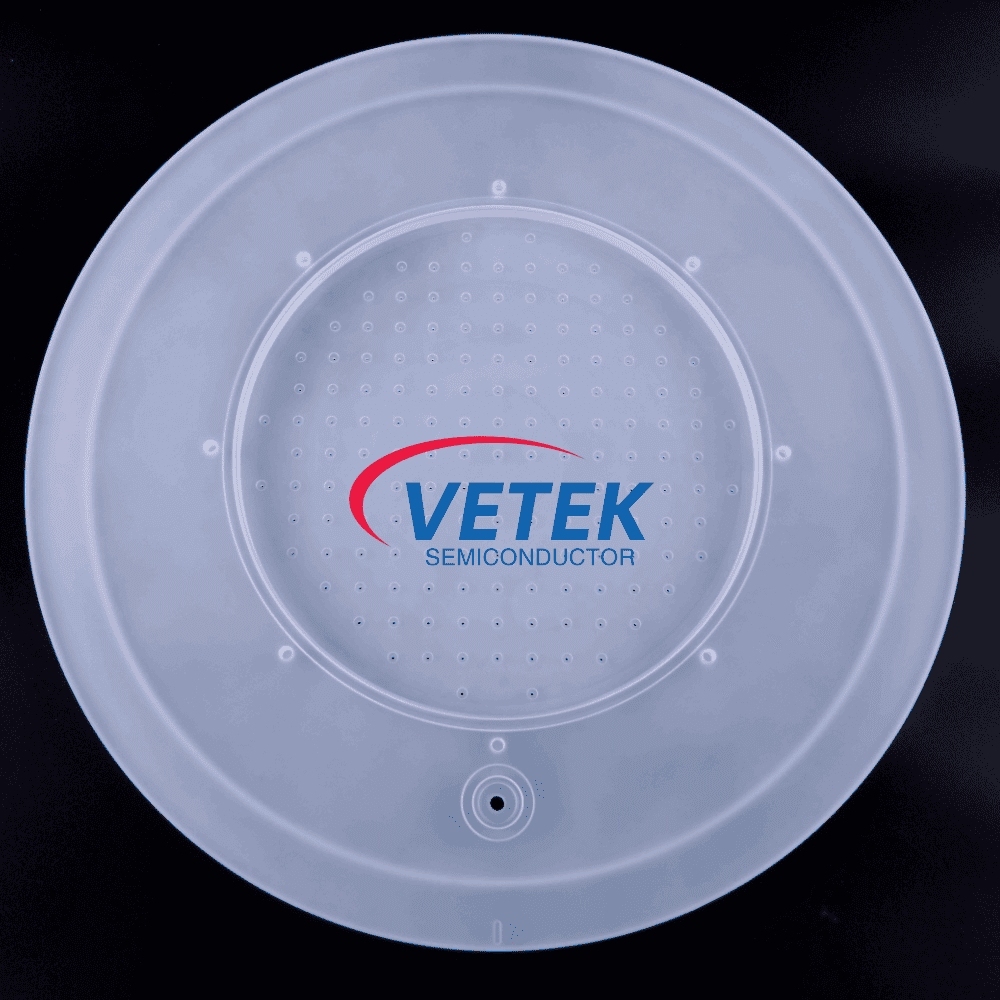
    The Quartz Shower Head, also known as a Quartz Gas Distribution Plate, is a critical component used in semiconductor thin-film deposition processes such as CVD(Chemical Vapor Deposition), PECVD (Plasma-Enhanced CVD),and ALD (Atomic Layer Deposition). Made from high-purity fused quartz, this component ensures ultra-low contamination and excellent thermal stability, enabling precise gas delivery and uniform film growth across the wafer surface. Looking forward to your further consultation.
  • CMP Polishing Slurry

    CMP Polishing Slurry

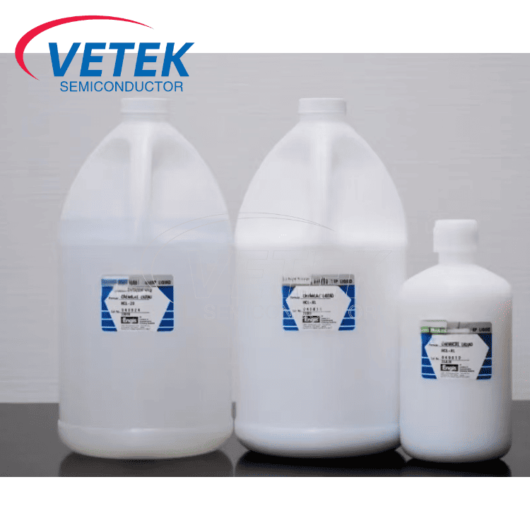
    CMP polishing slurry (Chemical Mechanical Polishing Slurry) is a high-performance material used in semiconductor manufacturing and precision material processing. Its core function is to achieve fine flatness and polishing of the material surface under the synergistic effect of chemical corrosion and mechanical grinding to meet the flatness and surface quality requirements at the nano level. Looking forward to your further consultation.
  • Large sized resistance heating SiC crystal growth furnace

    Large sized resistance heating SiC crystal growth furnace

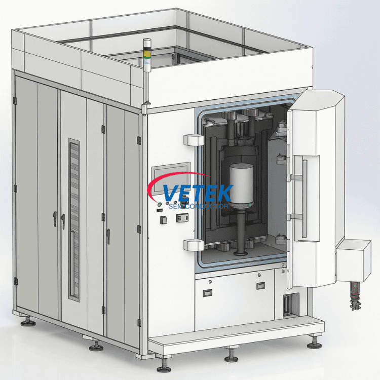
    Silicon carbide crystal growth is a core process in the manufacturing of high-performance semiconductor devices. The stability, precision, and compatibility of crystal growth equipment directly determine the quality and yield of silicon carbide ingots. Based on the characteristics of Physical Vapor Transport (PVT) technology, Veteksemi has developed a resistance heating furnace for silicon carbide crystal growth, enabling stable growth of 6-inch, 8-inch, and 12-inch silicon carbide crystals with full compatibility with conductive, semi-insulating, and N-type material systems. Through precise control of temperature, pressure, and power, it effectively reduces crystal defects such as EPD (Etch Pit Density) and BPD (Basal Plane Dislocation), while featuring low energy consumption and a compact design to meet the high standards of industrial large-scale production.

Send Inquiry

X
We use cookies to offer you a better browsing experience, analyze site traffic and personalize content. By using this site, you agree to our use of cookies. Privacy Policy
RejectAccept