
Products

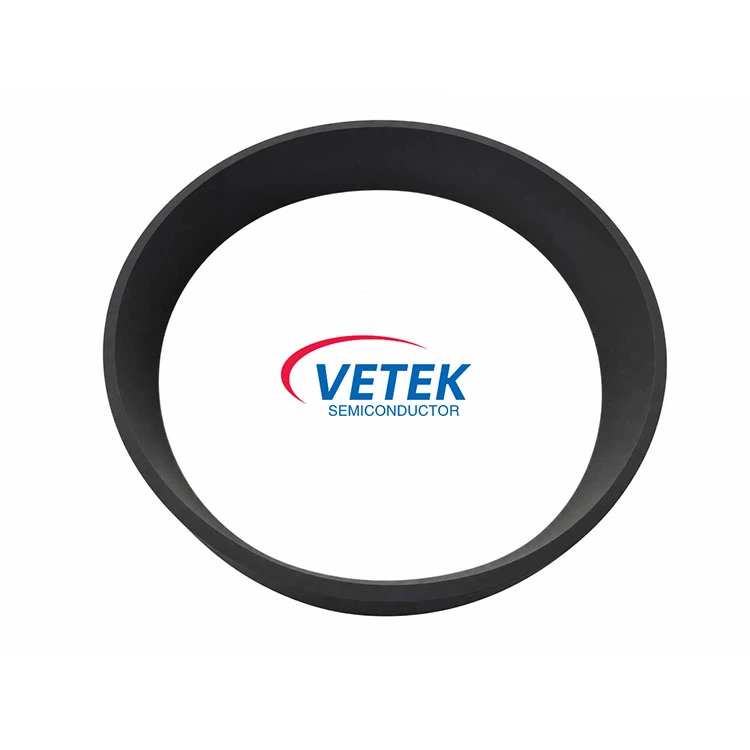
China Focus ring plasma etching Manufacturer, Supplier, Factory

We now have a skilled, performance team to supply good quality services for our consumer. We often follow the tenet of customer-oriented, details-focused for Focus ring plasma etching, Plasma etching equipment, Plasma etching process, Plasma etching device, Vetek plasma etching focus ring, Our solutions are widely recognized and reliable by users and can satisfy continuously acquiring economic and social needs.
Focus ring plasma etching, Our company adheres to the spirit of "lower costs, higher quality, and making more benefits for our clients". Employing talents from the same line and adhering to the principle of "honesty, good faith, real thing and sincerity", our company hopes to gain common development with clients from both at home and abroad!
Hot Products

  • CVD SiC Focus Ring

    CVD SiC Focus Ring

    VeTek Semiconductor is a leading domestic manufacturer and supplier of CVD SiC focus rings, dedicated to providing high-performance, high-reliability product solutions for the semiconductor industry. VeTek Semiconductor's CVD SiC focus rings use advanced chemical vapor deposition (CVD) technology, have excellent high temperature resistance, corrosion resistance and thermal conductivity, and are widely used in semiconductor lithography processes. Your inquiries are always welcome.
  • Three-Piece Graphite Crucibles

    Three-Piece Graphite Crucibles

    For demanding semiconductor crystal growth applications, the VETEK three‑piece graphite crucible delivers the stability, purity, and thermal evenness that the process requires. Made from high‑grade isostatic graphite—with optional SiC, TaC, or PyC coatings—its split design isn’t just for convenience. It actively reduces thermal stress, makes maintenance faster, and keeps performing cycle after cycle.
  • PZT Piezoelectric Wafers (PZT on Si/SOI)

    PZT Piezoelectric Wafers (PZT on Si/SOI)

    As the demand for high-sensitivity and low-power MEMS transducers grows with the expansion of 5G communications, precision medical devices, and smart wearables, our PZT on Si/SOI wafers provide a critical material solution. Utilizing advanced thin-film deposition processes such as Sol-gel or sputtering, we achieve exceptional consistency and superior piezoelectric performance on silicon substrates. These wafers serve as the fundamental core for electromechanical energy conversion.
  • MAX Phase Nanopowder

    MAX Phase Nanopowder

    Veteksemi’s Semiconductor MAX phase nanopowder offers exceptional thermal and electrical properties, ideal for advanced electronics and materials science applications. With superior oxidation resistance and high-temperature stability, Veteksemi's nanopowder is the perfect solution for innovative semiconductor technologies.
  • High purity CVD SiC raw material

    High purity CVD SiC raw material

    High purity CVD SiC raw material prepared by CVD is the best source material for silicon carbide crystal growth by physical vapor transport. The density of High purity CVD SiC raw material supplied by VeTek Semiconductor is higher than that of small particles formed by spontaneous combustion of Si and C-containing gases, and it does not require a dedicated sintering furnace and has a nearly constant evaporation rate. It can grow extremely high quality SiC single crystals. Looking forward to your inquiry.
  • C/C Composite Crucible

    C/C Composite Crucible

    Designed for the harsh environment of silicon single crystal production, the C/C Composite Crucible is an indispensable component of the semiconductor silicon single crystal production process.

Send Inquiry

X
We use cookies to offer you a better browsing experience, analyze site traffic and personalize content. By using this site, you agree to our use of cookies.Privacy Policy