
Products

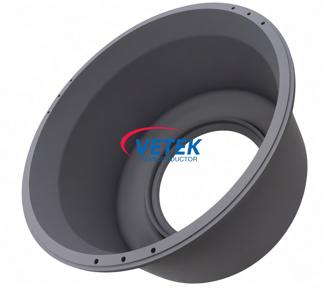
China CVD SiC Coated Graphite Outer Heat Shield, CZ Silicon Crystal Growth, Outer Flow Guide, 300mm Silicon Crystal Furnace, Graphite Thermal Shield Manufacturer, Supplier, Factory

"Control the standard by the details, show the toughness by quality". Our firm has strived to establish a highly efficient and stable workers workforce and explored an effective high-quality management system for CVD SiC Coated Graphite Outer Heat Shield, CZ Silicon Crystal Growth, Outer Flow Guide, 300mm Silicon Crystal Furnace, Graphite Thermal Shield, We now have substantial goods source and also the rate is our advantage. Welcome to inquire about our merchandise.
CVD SiC Coated Graphite Outer Heat Shield, CZ Silicon Crystal Growth, Outer Flow Guide, 300mm Silicon Crystal Furnace, Graphite Thermal Shield, We pay high attention to customer service, and cherish every customer. We have now maintained a strong reputation in the industry for many years. We're honest and work on building a long-term relationship with our customers.
Hot Products

  • SiC Coating Susceptor

    SiC Coating Susceptor

    Vetek Semiconductor focuses on the research and development and industrialization of CVD SiC coating and CVD TaC coating. Taking SiC coating susceptor as an example, the product is highly processed with high precision, dense CVD SIC coating, high temperature resistance and strong corrosion resistance. Your inquiry into us is welcome.
  • Pyrolytic Graphite Coated Graphite Elements

    Pyrolytic Graphite Coated Graphite Elements

    VeTek Semiconductor is a leading supplier of customized Pyrolytic Graphite Coated Graphite Elements in China. The Pyrolytic Graphite Coated Graphite Elements we provide have a dense surface structure, high purity and good high temperature resistance. VeTek Semiconductor is committed to establishing long-term strategic partnerships with customers to promote technological innovation and industrial development.
  • Semiconductor thermal spraying technology

    Semiconductor thermal spraying technology

    Vetek Semiconductor Semiconductor thermal spraying technology is an advanced process that sprays materials in a molten or semi-molten state onto the surface of a substrate to form a coating. This technology is widely used in the field of semiconductor manufacturing, mainly used to create coatings with specific functions on the surface of the substrate, such as conductivity, insulation, corrosion resistance, and oxidation resistance. The main advantages of thermal spraying technology include high efficiency, controllable coating thickness, and good coating adhesion, making it particularly important in the semiconductor manufacturing process that requires high precision and reliability. Looking forward to your inquiry.
  • PSS Etching Carrier Plate for Semiconductor

    PSS Etching Carrier Plate for Semiconductor

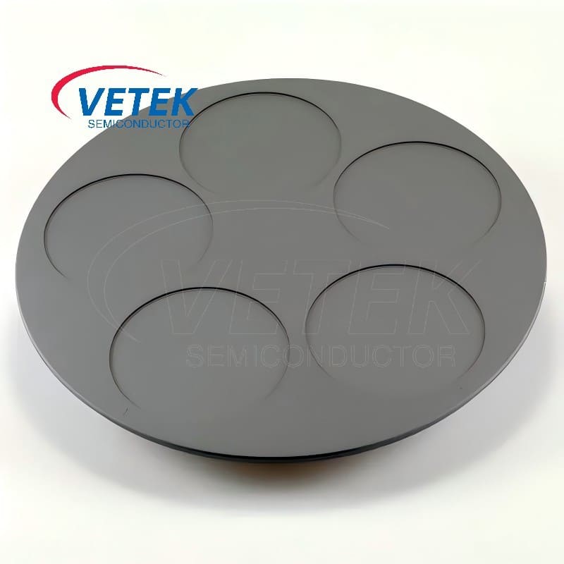
    VeTek Semiconductor's PSS Etching Carrier Plate for Semiconductor is a high-quality, ultra-pure graphite carrier designed for wafer handling processes. Our carriers have excellent performance and can perform well in harsh environments, high temperatures and harsh chemical cleaning conditions. Our products are widely used in many European and American markets, and we look forward to becoming your long-term partner in China.You are welcome to come to China to visit our factory and learn more about our technology and products.
  • SiC Coated Graphite Susceptor for MOCVD

    SiC Coated Graphite Susceptor for MOCVD

    VeTek Semiconductor is a leading manufacturer and supplier of SiC Coated Graphite Susceptor for MOCVD in China, specializing in SiC coating applications and epitaxial semiconductor products for the semiconductor industry. Our MOCVD SiC coated graphite susceptors offer competitive quality and pricing, serving markets across Europe and America. We are committed to becoming your long-term, trusted partner in advancing semiconductor manufacturing.
  • Ion Beam Sputter sources grid

    Ion Beam Sputter sources grid

    Ion beam is mainly used for ion etching, ion coating and plasma injection. The role of the Ion Beam Sputter sources grid is to dissect the ions and accelerate them to the required energy. Vetek Semiconductor provides high purity graphite ion beam Ion Beam Sputter sources grid for optical lens ion beam polishing, semiconductor wafer modification, etc. Welcome to inquire about customized products.

Send Inquiry

X
We use cookies to offer you a better browsing experience, analyze site traffic and personalize content. By using this site, you agree to our use of cookies. Privacy Policy
RejectAccept