
Products

China Wafer handling robot Manufacturer, Supplier, Factory

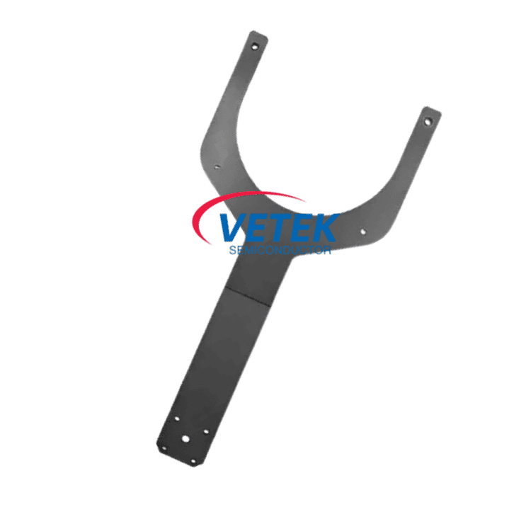
We depend on sturdy technical force and continually create sophisticated technologies to meet the demand of Wafer handling robot, Silicon carbide robot arm, SiC Robot Arm, SiC coated robotic arm, Semiconductor robot arm, Top quality, timely company and Aggressive cost, all win us a superior fame in xxx field despite the international intense competition.
Wafer handling robot, Based on our automatic production line, steady material purchase channel and quick subcontract systems have been built in mainland China to meet customer's wider and higher requirement in recent years. We have been looking forward to cooperating with more clients worldwide for common development and mutual benefit!Your trust and approval are the best reward for our efforts. Keeping honest, innovative and efficient, we sincerely expect that we can be business partners to create our brilliant future!

Hot Products

  • Porous Ceramic Vacuum Chuck

    Porous Ceramic Vacuum Chuck

    Vetek Semiconductor's Porous Ceramic Vacuum Chuck is made of silicon carbide ceramic (SiC) material, which has excellent high temperature resistance, chemical stability and mechanical strength. It is an indispensable core component in the semiconductor process. Welcome your further inquiries.
  • SiC Ceramic Seal Ring

    SiC Ceramic Seal Ring

    As a large-scale factory and supplier of SiC Ceramic Seal Ring products in China, VeTek Semiconductor SiC Ceramic Seal Ring has a wide range of applications in the industrial field due to its excellent thermal conductivity, outstanding chemical and corrosion resistance, and high strength and stiffness. Welcome your further inquiries.
  • Physical Vapor Deposition

    Physical Vapor Deposition

    Vetek semiconductor Physical Vapor Deposition (PVD) is an advanced process technology widely used in surface treatment and thin film preparation. PVD technology uses physical methods to directly transform materials from solid or liquid to gas and form a thin film on the surface of the target substrate. This technology has the advantages of high precision, high uniformity and strong adhesion, and is widely used in semiconductors, optical devices, tool coatings and decorative coatings. Welcome to discuss with us!
  • Porous SiC Ceramic Plate

    Porous SiC Ceramic Plate

    Our porous SiC ceramic plates are porous ceramic materials made of silicon carbide as the main component and processed by special processes. They are indispensable materials in semiconductor manufacturing, chemical vapor deposition (CVD) and other processes.
  • Halfmoon for LPE Reaction Chamber

    Halfmoon for LPE Reaction Chamber

    The Halfmoon is a graphite component used inside LPE SiC reactors, mainly installed around the chamber hot zone. Although it does not directly contact the wafer, it still plays a role in gas flow stability and reactor operation during epitaxial growth.To handle high temperature and reactive process conditions, the component is usually protected with CVD SiC coating, while TaC coating is also available for some applications. VETEK also supplies graphite felt insulation and other coated graphite parts for SiC epitaxy systems.
  • PZT Piezoelectric Wafers (PZT on Si/SOI)

    PZT Piezoelectric Wafers (PZT on Si/SOI)

    As the demand for high-sensitivity and low-power MEMS transducers grows with the expansion of 5G communications, precision medical devices, and smart wearables, our PZT on Si/SOI wafers provide a critical material solution. Utilizing advanced thin-film deposition processes such as Sol-gel or sputtering, we achieve exceptional consistency and superior piezoelectric performance on silicon substrates. These wafers serve as the fundamental core for electromechanical energy conversion.

Send Inquiry

X
We use cookies to offer you a better browsing experience, analyze site traffic and personalize content. By using this site, you agree to our use of cookies.Privacy Policy