
Products

China SiC Process Tube Manufacturer, Supplier, Factory

Our purpose will be to fulfill our shoppers by offering golden assistance, fantastic price and high quality for SiC Process Tube, Silicon Carbide Process Tube, SiC Tube for Semiconductor, High Temperature SiC Tube, SiC Processing Equipment, All products are manufactured with advanced equipment and strict QC procedures in order to ensure high quality. Welcome customers new and old to contact us for business cooperation.
SiC Process Tube, We welcome an opportunity to do business with you and hope to have pleasure in attaching further details of our products. Excellent quality, competitive price, punctual delivery and dependable service can be guaranteed. For further inquires be sure to do not hesitate to contact us.

Hot Products

  • SiC Coating Epi susceptor

    SiC Coating Epi susceptor

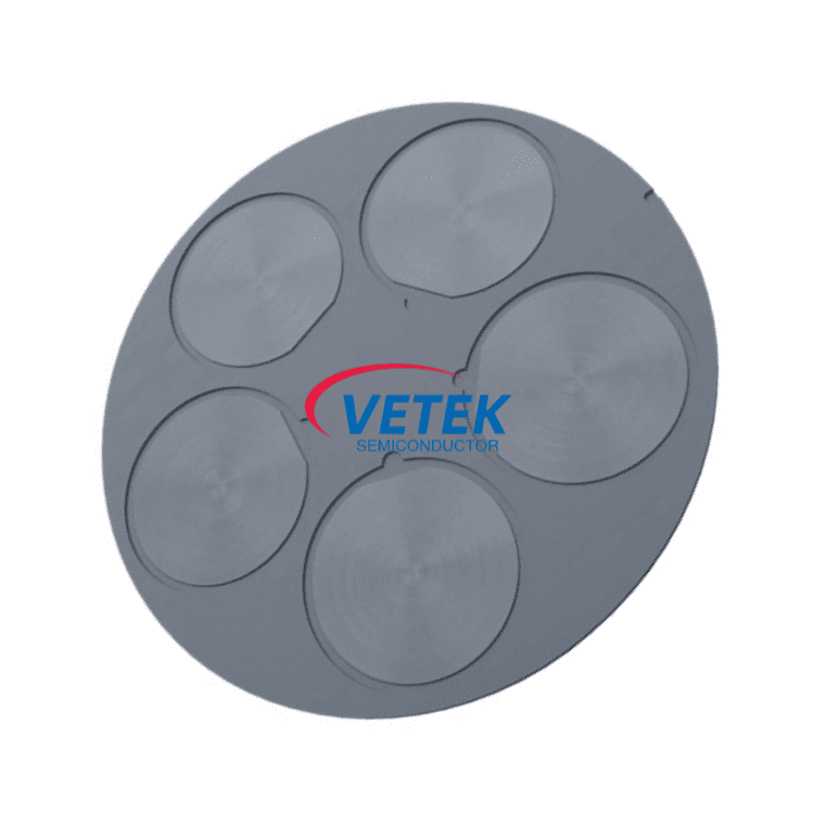
    VeTek Semiconductor is a leading manufacturer, innovator of SiC Coating Epi Susceptor products in China. For many years, we have been focusing on various SiC Coating products such as SiC Coating Epi Susceptor, SiC coating ALD susceptor, etc. Welcome your further consultation.
  • CVD SiC Coated Ceiling

    CVD SiC Coated Ceiling

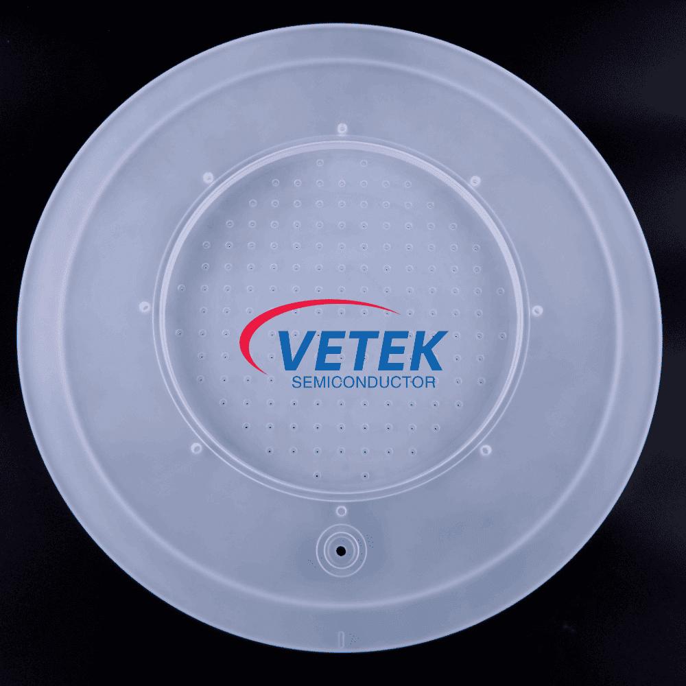
    VeTek Semiconductor's CVD SiC coated ceiling has excellent properties such as high temperature resistance, corrosion resistance, high hardness, and low thermal expansion coefficient, making it an ideal material choice in semiconductor manufacturing. As a China leading CVD SiC coated ceiling manufacturer and supplier, VeTek semiconductor looks forward to your consultation.
  • TaC Coated Graphite Susceptor

    TaC Coated Graphite Susceptor

    VeTek Semiconductor’s TaC Coated Graphite Susceptor uses chemical vapor deposition(CVD) method to prepare tantalum carbide coating on the surface of graphite parts. This process is the most mature and has the best coating properties. TaC Coated Graphite Susceptor can extend the service life of graphite components, inhibit the migration of graphite impurities, and ensure the quality of epitaxy.We are looking forward to your inquiry.
  • Chemical Vapor Deposition Process Solid SiC Edge Ring

    Chemical Vapor Deposition Process Solid SiC Edge Ring

    VeTek Semiconductor has always been committed to the research and development and manufacturing of advanced semiconductor materials. Today, VeTek Semiconductor has made great progress in Chemical Vapor Deposition Process Solid SiC Edge Ring products and is able to provide customers with highly customized solid SiC edge rings. Solid SiC edge rings provide better etching uniformity and precise wafer positioning when used with an electrostatic chuck, ensuring consistent and reliable etching results. Looking forward to your inquiry and becoming each other's long-term partners.
  • Semiconductor Quartz Crucible

    Semiconductor Quartz Crucible

    Veteksemicon semiconductor-grade quartz crucibles are key consumables in the Czochralski single crystal growth process. With extreme purity and superior thermal stability as our core focus, we are committed to providing customers with high-quality products that exhibit stable performance and excellent resistance to crystallization under high temperature and high pressure environments. This ensures the quality of the crystal rods from the source, helping semiconductor silicon wafer manufacturing achieve higher yields and better cost-effectiveness.
  • Large sized resistance heating SiC crystal growth furnace

    Large sized resistance heating SiC crystal growth furnace

    Silicon carbide crystal growth is a core process in the manufacturing of high-performance semiconductor devices. The stability, precision, and compatibility of crystal growth equipment directly determine the quality and yield of silicon carbide ingots. Based on the characteristics of Physical Vapor Transport (PVT) technology, Veteksemi has developed a resistance heating furnace for silicon carbide crystal growth, enabling stable growth of 6-inch, 8-inch, and 12-inch silicon carbide crystals with full compatibility with conductive, semi-insulating, and N-type material systems. Through precise control of temperature, pressure, and power, it effectively reduces crystal defects such as EPD (Etch Pit Density) and BPD (Basal Plane Dislocation), while featuring low energy consumption and a compact design to meet the high standards of industrial large-scale production.

Send Inquiry

X
We use cookies to offer you a better browsing experience, analyze site traffic and personalize content. By using this site, you agree to our use of cookies.Privacy Policy
RejectAccept