


QR Code

Products
Contact Us


Fax
+86-579-87223657

E-mail

Address
Wangda Road, Ziyang Street, Wuyi County, Jinhua City, Zhejiang Province, China


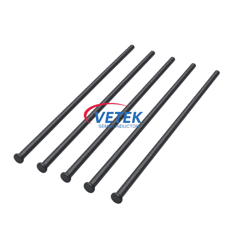
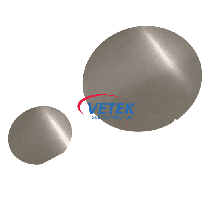
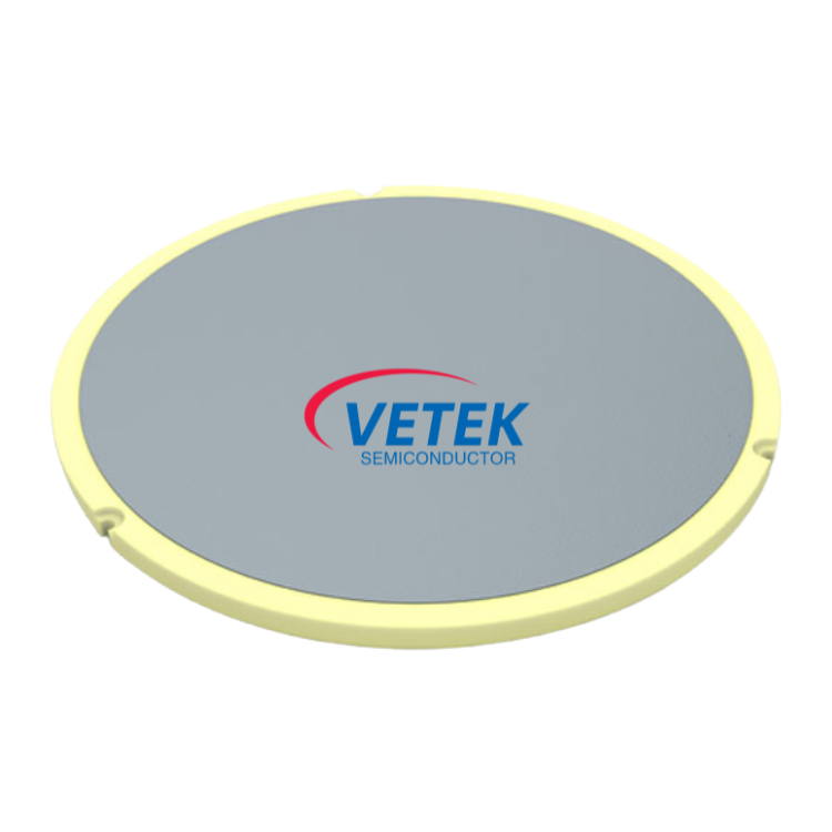
We goal to see good quality disfigurement within the manufacturing and provide the most effective support to domestic and overseas shoppers wholeheartedly for Wafer Lift Pin, AMAT 0200-03201, Thin Wall SiC Coated Graphite, CVD SiC Coating, 300mm Epitaxy Parts, Accurate process devices, Advanced Injection Molding Equipment, Equipment assembly line, labs and software progress are our distinguishing feature.
Wafer Lift Pin, Based on our automatic production line, steady material purchase channel and quick subcontract systems have been built in mainland China to meet customer's wider and higher requirement in recent years. We have been looking forward to cooperating with more clients worldwide for common development and mutual benefit!Your trust and approval are the best reward for our efforts. Keeping honest, innovative and efficient, we sincerely expect that we can be business partners to create our brilliant future!


+86-579-87223657
Wangda Road, Ziyang Street, Wuyi County, Jinhua City, Zhejiang Province, China