
Products

China PVD process Manufacturer, Supplier, Factory

We know that we only thrive if we could guarantee our combined price tag competiveness and quality advantageous at the same time for PVD process, CVD SiC Coated Ceiling, SiC Coating, Physical Vapor Deposition, Physical Vapor Deposition process, Our ultimate goal is to rank as a top brand and to lead as a pioneer in our field. We are sure our successful experience in tool production will win customer's trust, Wish to co-operate and co-create a better future with you!
PVD process, Now, we are trying to enter new markets where we do not have a presence and developing the markets we have now the already penetrated. On account of superior quality and competitive price , we'll be the market leader, please don??¥t hesitate to contact us by phone or email, if you are interested in any of our goods.

Hot Products

  • SiC Coating Set Disc

    SiC Coating Set Disc

    VeTek Semiconductor is top manufacturer of CVD SiC coatings in China, offers SiC Coating Set Disc in Aixtron MOCVD Reactors. These SiC Coating Set Disc are crafted using high purity graphite and feature a CVD SiC coating with impurity below 5ppm. Your inquiry is welcomed.
  • TaC Coating Plate

    TaC Coating Plate

    Designed with precision and engineered to perfection, Vetek Semiconductor's TaC Coating Plate is specifically tailored for various applications in silicon carbide (SiC) single crystal growth processes.The TaC Coating Plate's precise dimensions and robust construction make it easy to integrate into existing systems, ensuring seamless compatibility and efficient operation. Its reliable performance and high-quality coating contribute to consistent and uniform results in SiC crystal growth applications.We are committed to providing quality products at competitive prices and look forward to being your long-term partner in China.
  • CVD TaC Coated Graphite Ring

    CVD TaC Coated Graphite Ring

    The CVD TaC Coated Graphite Ring by Veteksemicon is engineered to meet the extreme demands of semiconductor wafer processing. Utilizing Chemical Vapor Deposition (CVD) technology, a dense and uniform Tantalum Carbide (TaC) coating is applied to high-purity graphite substrates, achieving exceptional hardness, wear resistance, and chemical inertness. In semiconductor fabrication, the CVD TaC Coated Graphite Ring is widely used in MOCVD, etching, diffusion, and epitaxial growth chambers, serving as a key structural or sealing component for wafer carriers, susceptors, and shielding assemblies. Looking forward to your further consultation.
  • Aluminum Nitride ceramic Disc

    Aluminum Nitride ceramic Disc

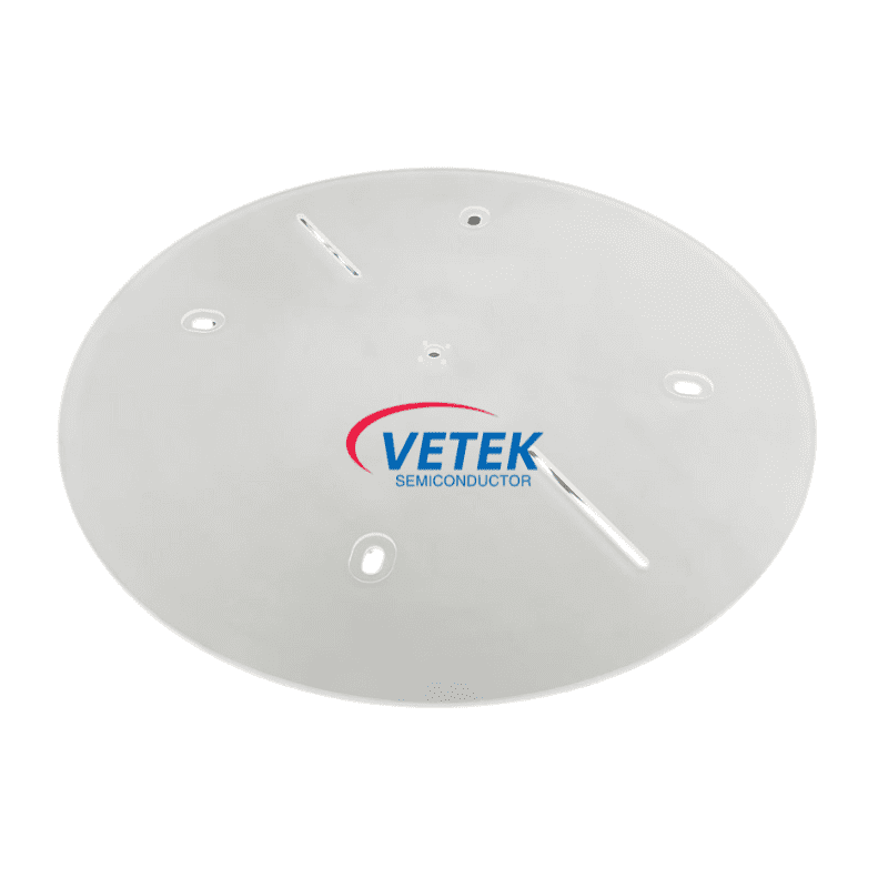
    Vetek Semiconductor aluminum nitride ceramics disc is a high-performance material known for its excellent properties of high thermal conductivity & electrical insulation, especially suitable for demanding electrical applications. Aluminum nitride ceramic discs are stable at high temperatures in a variety of inert environments. Welcome to communicate with us.
  • TaC Coated Deflector Ring

    TaC Coated Deflector Ring

    VeTek Semiconductor's TaC Coated Deflector Ring is a highly specialized component designed for SiC crystal growth processes. The TaC coating provides excellent high temperature resistance and chemical inertness to cope with the high temperatures and corrosive environments during crystal growth process. This ensures stable performance and long life of the component, reducing the frequency of replacement and downtime. We are committed to providing quality products at competitive prices and look forward to being your long-term partner in China.Welcome to consult at any time.
  • Silicon Cassette Boat

    Silicon Cassette Boat

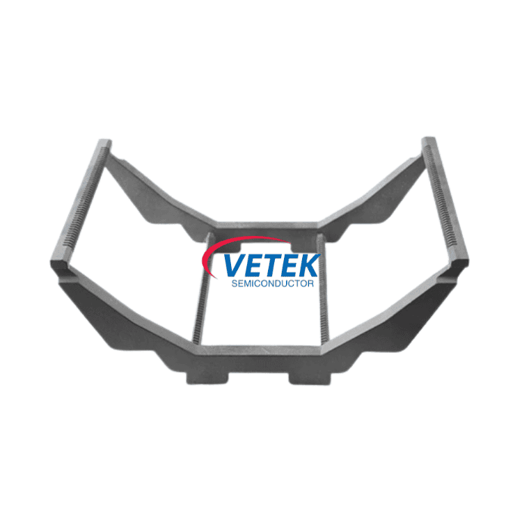
    The Silicon Cassette Boat from Veteksemicon is a precision-engineered wafer carrier developed specifically for high-temperature semiconductor furnace applications, including oxidation, diffusion, drive-in, and annealing. Fabricated from ultra-high-purity silicon and finished to advanced contamination-control standards, it provides a thermally stable, chemically inert platform that closely matches the properties of silicon wafers themselves. This alignment minimizes thermal stress, reduces slip and defect formation, and ensures exceptionally uniform heat distribution throughout the batch

Send Inquiry

X
We use cookies to offer you a better browsing experience, analyze site traffic and personalize content. By using this site, you agree to our use of cookies.Privacy Policy