News

News

We are glad to share with you about the results of our work, company news,and give you timely developments and personnel appointment and removal conditions.
How Does Semiconductor Quartz Crucible Performance Affect Crystal Growth Stability?20 2026-04

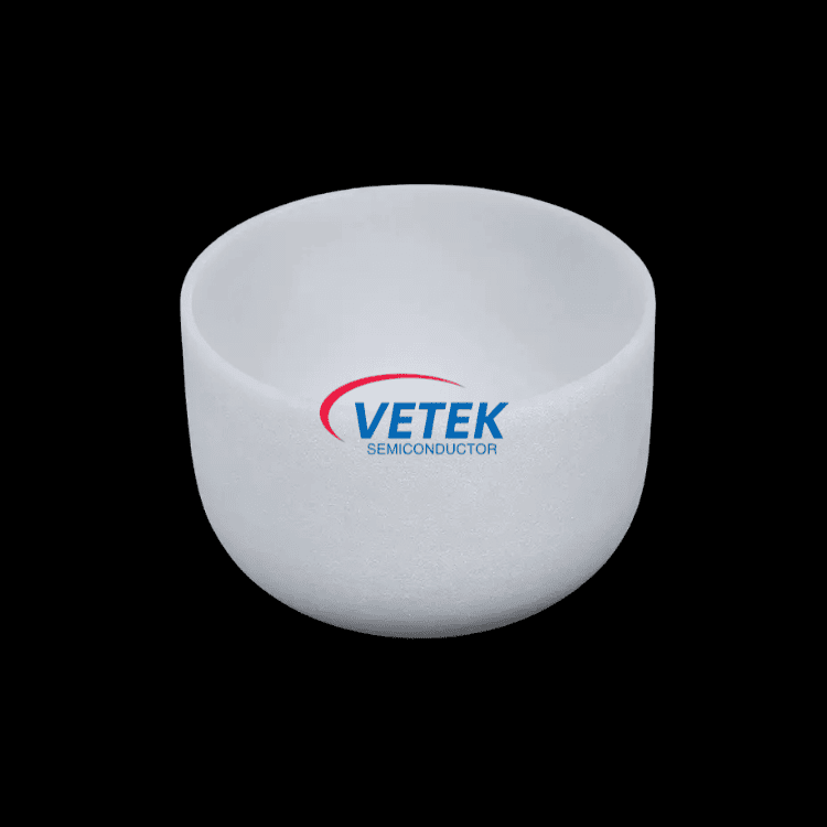
How Does Semiconductor Quartz Crucible Performance Affect Crystal Growth Stability?

Choosing the right Semiconductor Quartz Crucible is not a minor purchasing detail. It directly affects melt cleanliness, thermal stability, crystal pulling consistency, yield control, and the service rhythm of the entire growth line.
What Makes High Purity Graphite Powder Essential for Advanced Semiconductor and Industrial Applications10 2026-02

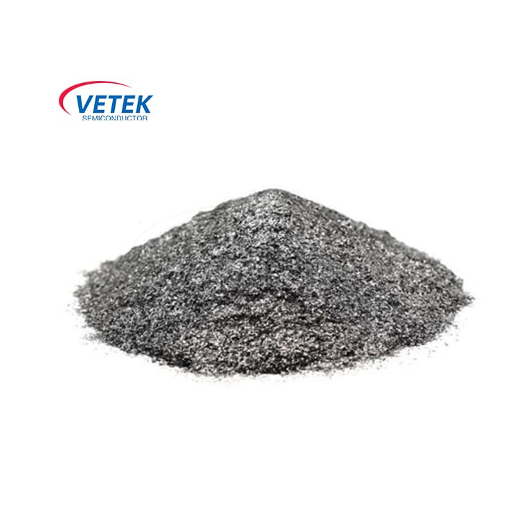
What Makes High Purity Graphite Powder Essential for Advanced Semiconductor and Industrial Applications

High purity graphite powder has become a critical material across semiconductor manufacturing, photovoltaic production, advanced ceramics, and high-temperature industrial processes. But what exactly defines high purity graphite powder, and why does it outperform standard graphite materials in demanding environments?
What Is a Tantalum Carbide Coating Ring and Why Is It Critical in Semiconductor Processing09 2026-02

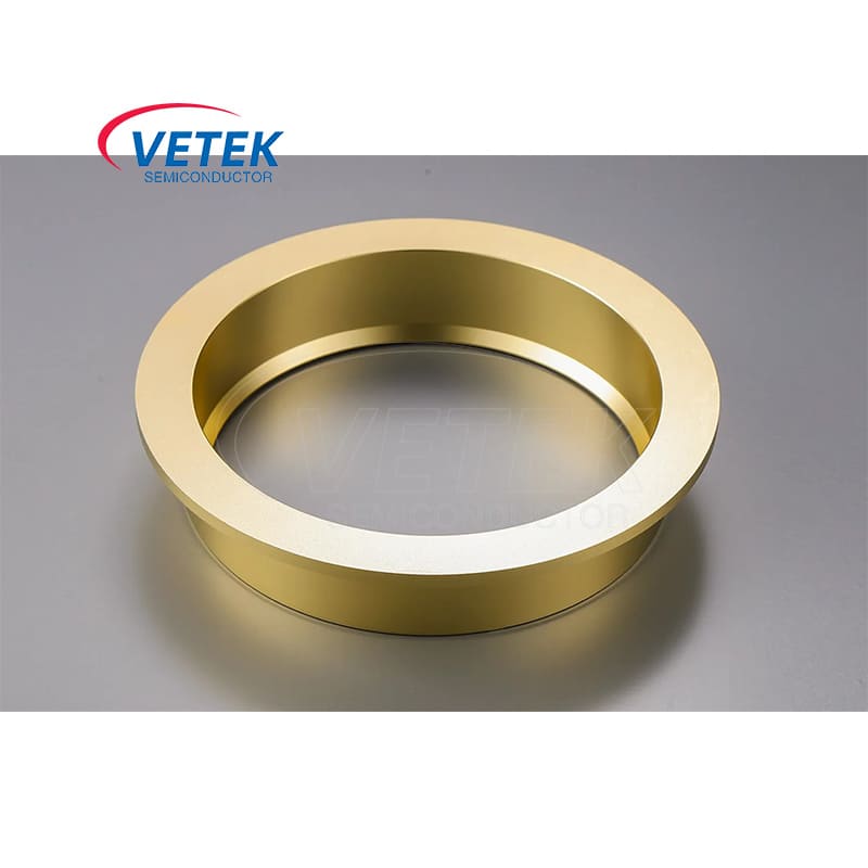
What Is a Tantalum Carbide Coating Ring and Why Is It Critical in Semiconductor Processing

As semiconductor manufacturing advances toward higher precision, higher temperatures, and more aggressive plasma environments, material selection for critical components becomes increasingly important. The Tantalum Carbide Coating Ring has emerged as a key solution for plasma-facing and high-temperature applications due to its exceptional hardness, thermal stability, and chemical resistance. This article provides a comprehensive, in-depth exploration of what a tantalum carbide coating ring is, how it works, why it outperforms traditional materials, and why leading manufacturers trust solutions from VeTek semiconductor.
What Makes SiC Ceramics Wafer Boat Essential for Modern Semiconductor Manufacturing16 2026-01

What Makes SiC Ceramics Wafer Boat Essential for Modern Semiconductor Manufacturing

Silicon carbide (SiC) ceramics wafer boats have emerged as indispensable tools in modern semiconductor and photovoltaic fabrication environments. These advanced components play a pivotal role in wafer processing steps such as oxidation, diffusion, epitaxial growth, and chemical vapor deposition.
What Are the Advantages of TaC Coating Rings in Semiconductor Applications07 2026-01

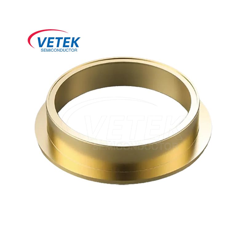
What Are the Advantages of TaC Coating Rings in Semiconductor Applications

TaC (Tantalum Carbide) coating rings are integral components in semiconductor manufacturing, especially for equipment exposed to harsh environments. This blog explores the benefits of using TaC coating rings, their application in semiconductor processes, and why VeTek's TaC coating solutions are the best choice for industry professionals. By diving into their performance, cost-effectiveness, and durability, this article highlights the role these advanced coatings play in enhancing semiconductor device quality.
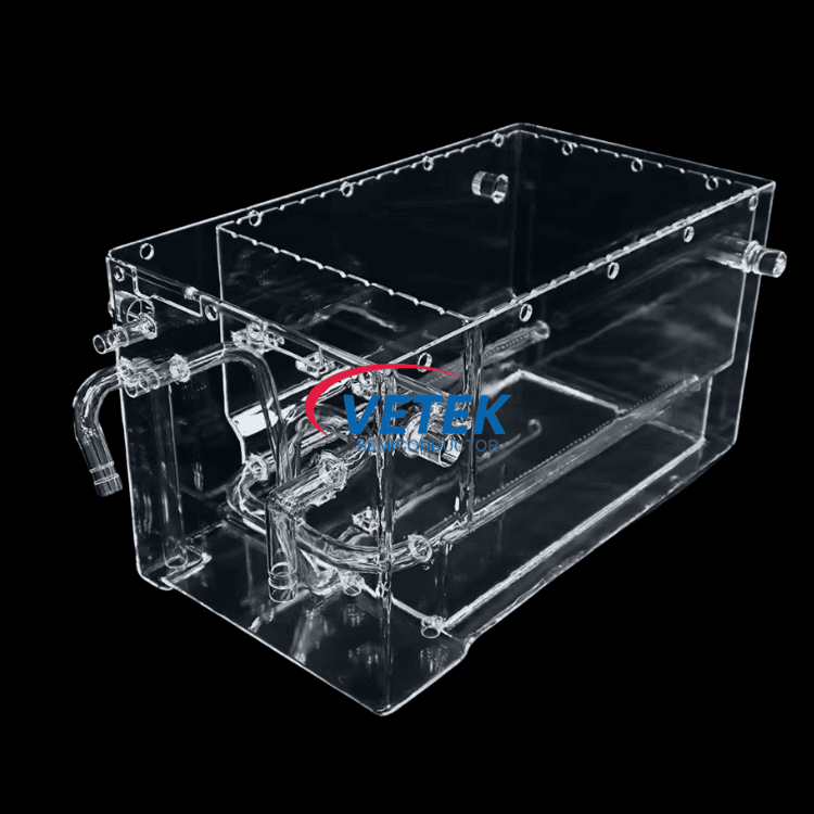
What Makes a High-Purity Quartz Bath Essential for Advanced Semiconductor Processes22 2025-12

What Makes a High-Purity Quartz Bath Essential for Advanced Semiconductor Processes

In semiconductor, solar cell, and microelectronics manufacturing, precision wet processing like wafer cleaning, etching, and surface preparation demand materials and equipment that ensure ultra-high purity, thermal stability and corrosion resistance. A High-Purity Quartz Bath provides these attributes with synthetic fused quartz construction, making it a cornerstone of modern fabrication environments.
Why Should High Purity SiC Powder Be the Heart of Your Next EV Power System17 2025-11

Why Should High Purity SiC Powder Be the Heart of Your Next EV Power System

For two decades at the forefront of technological innovation, I’ve seen components come and go. But few have generated as sustained a buzz as High Purity SiC Powder. It’s not just another material; it’s the foundational element pushing the boundaries of what’s possible in electric vehicles.
‌VETEK will participate in the 2025 SEMICON Europa exhibition in Munich Germany10 2025-11

‌VETEK will participate in the 2025 SEMICON Europa exhibition in Munich Germany

‌The SEMICON Europa semiconductor exhibition in Munich, Germany, will be held in November in Europe. Hosted by SEMI (Semiconductor Equipment and Materials International), it has become one of the most influential global semiconductor industry equipment exhibitions and is one of the largest and most significant events in Europe
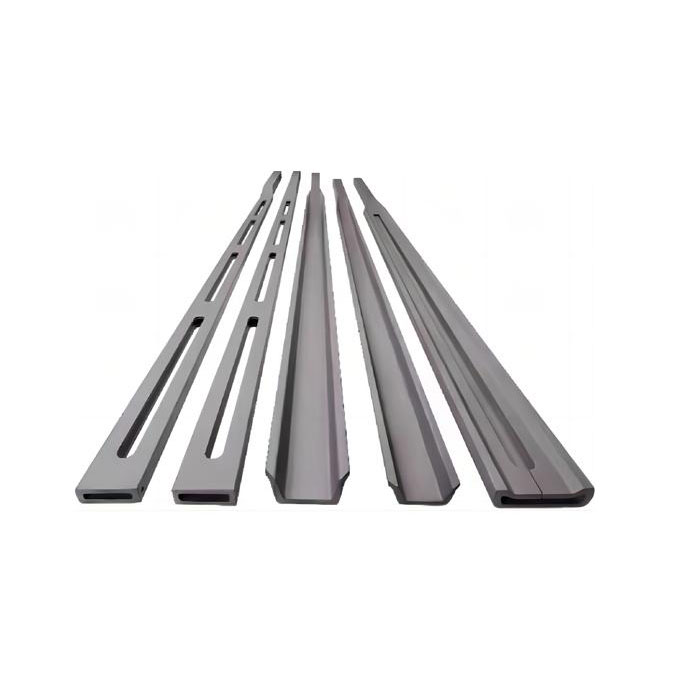
Can Silicon Carbide Ceramics Withstand Extreme Industrial Environments22 2025-10

Can Silicon Carbide Ceramics Withstand Extreme Industrial Environments

At VeTek Semiconductor, we've specialized in pushing the boundaries of what's possible with advanced Silicon Carbide Ceramics, developing grades specifically engineered to thrive where other materials falter.
Is Porous Graphite The Key To Faster Charging Batteries28 2025-08

Is Porous Graphite The Key To Faster Charging Batteries

We’ve all felt that moment of panic. Your phone battery is at 5%, you have minutes to spare, and every second plugged in feels like an eternity. What if the secret to ending this anxiety lies not in a completely new chemistry, but in reimagining a fundamental material within the battery itself? For two decades at the forefront of tech, I’ve seen trends come and go. But the buzz around Porous Graphite feels different. It isn't just an incremental step; it represents a fundamental shift in how we approach energy storage design.
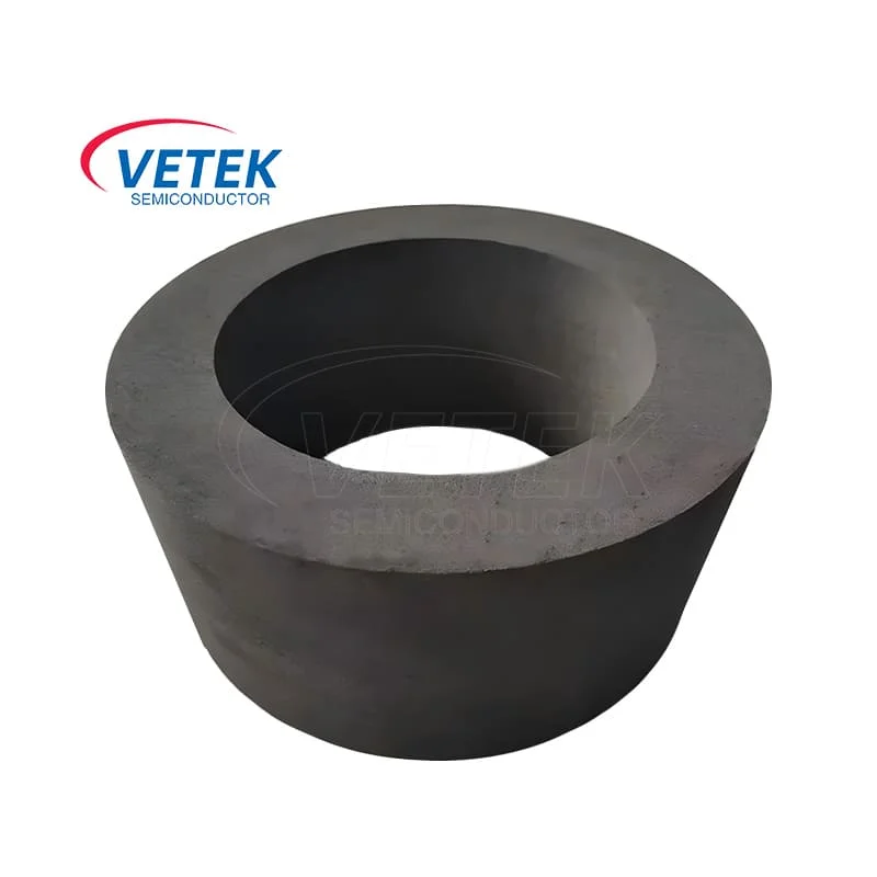
Can Isotropic Graphite Withstand Extreme Heat in High-Temperature Furnaces14 2025-08

Can Isotropic Graphite Withstand Extreme Heat in High-Temperature Furnaces

At VETEK, we’ve spent decades refining our isotropic graphite solutions for industries that demand reliability at soaring temperatures. Let’s dive into why this material is a top choice—and how our products outperform the competition.
Still worried about material performance in high-temperature environments?31 2025-07

Still worried about material performance in high-temperature environments?

Having worked in the semiconductor industry for over a decade, I understand firsthand how challenging material selection can be in high-temperature, high-power environments. It wasn't until I encountered VETEK's SiC Block that I finally found a truly reliable solution.
Veteksemicon shines at the 2025 Shanghai SEMICON International Exhibition26 2025-03

Veteksemicon shines at the 2025 Shanghai SEMICON International Exhibition

Veteksemicon shines at 2025 Shanghai SEMICON International Exhibition, leading the future of semiconductor industry with innovative technologies
Chip Manufacturing: Atomic Layer Deposition (ALD)16 2024-08

Chip Manufacturing: Atomic Layer Deposition (ALD)

In the semiconductor manufacturing industry, as device size continues to shrink, the deposition technology of thin film materials has posed unprecedented challenges. Atomic Layer Deposition (ALD), as a thin film deposition technology that can achieve precise control at the atomic level, has become an indispensable part of semiconductor manufacturing. This article aims to introduce the process flow and principles of ALD to help understand its important role in advanced chip manufacturing.
What is semiconductor epitaxy process?13 2024-08

What is semiconductor epitaxy process?

It is ideal to build integrated circuits or semiconductor devices on a perfect crystalline base layer. The epitaxy (epi) process in semiconductor manufacturing aims to deposit a fine single-crystalline layer, usually about 0.5 to 20 microns, on a single-crystalline substrate. The epitaxy process is an important step in the manufacture of semiconductor devices, especially in silicon wafer manufacturing.
What is the difference between epitaxy and ALD?13 2024-08

What is the difference between epitaxy and ALD?

The main difference between epitaxy and atomic layer deposition (ALD) lies in their film growth mechanisms and operating conditions. Epitaxy refers to the process of growing a crystalline thin film on a crystalline substrate with a specific orientation relationship, maintaining the same or similar crystal structure. In contrast, ALD is a deposition technique that involves exposing a substrate to different chemical precursors in sequence to form a thin film one atomic layer at a time.
X
We use cookies to offer you a better browsing experience, analyze site traffic and personalize content. By using this site, you agree to our use of cookies. Privacy Policy
RejectAccept