
Tech &  solutions

02 Selection Guide for Advanced Ceramic and Quartz Parts in Semiconductor Equipment: Materials, Failure, Customization and Procurement Overview

Industry

Semiconductor manufacturing (etch, thin film, diffusion, ion implant and other chamber parts)

Process

Material selection and replacement of chamber parts for etch, CVD/PVD, diffusion/oxidation, anneal, ion implant, etc.

Solution

Selection framework for quartz + alumina / AlN / Si₃N₄ / bulk SiC; boundary vs CVD coating solutions

Services

Material selection consulting, drawing-based customization, sample verification, purity and lot technical support

Results

• One “process environment → material role” mapping framework

• Clear quartz vs ceramic division; fewer mix-up errors

• Failure, customization and procurement paths drill down to sub-pages

• Two-way distinction and linking with graphite CVD SiC coating topic

The real question in chamber-part selection is often not “ceramics or quartz,” but: under the current temperature, corrosion, electrical and mechanical constraints, which material can control particles, lifetime and cost together. This article builds a unified selection framework for semiconductor advanced ceramics and quartz, explains their role split, a four-dimension assessment approach, and reading paths for failure, customization and procurement—and draws a clear line between bulk silicon carbide and graphite + CVD SiC coating.

1.Why Put Advanced Ceramics and Quartz in the Same Selection Framework?

Core Conclusion: The material systems differ, but the customer role and decision scene are the same: semiconductor equipment and fab engineers selecting chamber parts, replacing them and managing lifetime. One shared framework fits real workflow better than a “ceramics encyclopedia” or a “quartz encyclopedia.”

Quartz's core value is high purity, thermal stability and chemical inertness—common in diffusion furnace tubes, liners, boats, etch-chamber quartz rings and viewports. Ceramics cover regimes where quartz is weak—higher wear resistance, better electrical insulation, or temperatures and plasma exposure beyond quartz's comfort zone. Putting them on one page gives a single language for “should we change material.”

2.What Are the Roles of Ceramics and Quartz in the Chamber?

Core Conclusion: Quartz excels at high purity, optical/RF transmission and conventional high-temperature inert environments; ceramics excel at wear resistance, insulation, thermal matching and strong plasma exposure positions. Inside one chamber they often share roles—not a pure either/or.

Typical Roles of Quartz

Diffusion/oxidation tubes and liners, wafer boats, some etch rings and nozzles, viewports. Strengths: purity and chemical inertness. Weaknesses: plasma sputter wear (Mohs hardness ~7) and crystallization risk under long ultra-high-temperature exposure.

Typical Roles of Ceramics

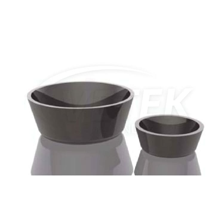
Alumina: cost-effective insulation and structural parts for mid/low-temperature duty. Aluminum nitride: high thermal conductivity and closer CTE match to silicon—often considered for electrostatic chuck upgrades. Silicon nitride: good strength and thermal shock resistance for positions with mechanical impact risk. Bulk silicon carbide: wear-critical parts in plasma environments (e.g. focus rings)—not the same technical path as “graphite + CVD SiC coating.”

If you care about CVD silicon carbide coating on graphite parts (thickness, uniformity, adhesion and deposition process), see the existing topic: Graphite Parts CVD Silicon Carbide Coating Topic. This cluster only discusses bulk ceramics and quartz parts and does not expand coating process details.

3.How to Select with a Temperature–Corrosion–Electrical–Mechanical Framework?

Core Conclusion: Do not fixate on a single parameter. First set the temperature window and corrosive medium, then whether insulation / thermal conductivity / RF transmission is required, and finally close with mechanical impact and machining cost. Selection is reusable only when all four dimensions land on checkable process descriptions.

A simplified engineering sequence:

1. Temperature: Is duty long above quartz's comfort zone or into crystallization-prone ranges? Is an AlN or SiC temperature band required?

2. Corrosion: Fluorine/chlorine plasma, wet HF, etc.—when etch rates between quartz and ceramics differ by an order of magnitude, material choice is often already locked.

3. Electrical: Must it insulate? Need high thermal conductivity matched to the wafer? Need optical/RF transmission (quartz window advantage)?

4. Mechanical: Impact, clamp preload, wall thickness and sharp corners—ceramic brittleness explains many early failures that look like “material problems” but are design problems.

Detailed comparison of the four ceramics: How to Select Semiconductor Advanced Ceramics: Engineer Comparison of Alumina, Aluminum Nitride, Silicon Nitride and Silicon Carbide; quartz purity and grades: How to Select Semiconductor Quartz Parts: Purity, Crystallization and Contamination Control of Fused and Synthetic Quartz.

4.Which Signals Matter First for Failure, Customization and Procurement?

Core Conclusion: Lifetime management starts by recognizing the failure mode: for quartz, crystallization and metal contamination; for ceramics, design stress concentration and plasma wear. Customization needs a drawing and verification checklist; procurement needs purity, lot consistency and failure-driven respec. Do not end the problem with “just replace the part.”

Failure Signals (Overview)

Quartz: crystallization tendency under long ≥1000°C duty, alkali-metal catalyzed crystallization, metal contamination from secondary processing pollution. Ceramics: stress concentration at sharp internal corners, uneven wall thickness causing sinter distortion and cracking, excessive bolt preload causing immediate fracture. Plasma positions: when quartz sputter loss accelerates, evaluate whether to move to bulk SiC or other more wear-resistant options.

Customization and Procurement Path (Overview)

At customization, write clearly: temperature/medium/cleanliness, critical dimensions and mounting, load direction, tolerance/roughness, volume and verification expectations. At procurement, be able to verify: purity methods, machining capability, lot consistency; after failure, use morphology and impurity data to revise the next specification—not to reorder the same part. Detailed steps: sub-pages C3–C5 on failure investigation path, custom machining points, and supplier and procurement verification.

5.Reading Path and Sub-page Navigation for This Cluster

Core Conclusion: The pillar page only builds the framework; detailed comparison, failure, customization and procurement live on sub-pages. Read the one most relevant to the current task first, then expand via internal links.

1. C1 How to select ceramics: Four-way comparison of alumina, AlN, Si₃N₄ and bulk SiC (including boundary vs coating solutions).

2. C2 How to select quartz: Fused/synthetic quartz, purity thresholds, crystallization and contamination control.

3. C3 Why parts fail: Investigation path for crystallization, plasma erosion, metal contamination and cracking.

4. C4 Custom machining: Drawing review, tolerance, AlN machining difficulty and quartz welding/polish notes.

5. C5 Supplier and procurement verification: Purity, lot consistency, using failure to revise the next specification.

6.FAQ

1. Can quartz and ceramics substitute for each other?

In a few scenarios replacement can be discussed (e.g. evaluating a ceramic option when a quartz ring wears too fast under plasma), but most roles are not interchangeable: optical/RF windows still lean quartz; strong-plasma wear positions lean bulk SiC and similar. Judge by the four-dimension framework—not by “more expensive is better.”

2. What is the difference between bulk SiC and graphite + CVD SiC coating?

Bulk SiC is the bulk material with no coating–substrate interface; graphite + CVD SiC is a coating solution focused on thickness uniformity, adhesion and deposition process. This cluster covers the former; the latter is in the Graphite Parts CVD Silicon Carbide Coating Topic.

3. Look at material datasheets first, or failure modes first?

Early selection: use the four-dimension framework to narrow materials. On a running line: recognize the failure mode first, then decide whether to change purity grade, change material, or change design/mounting.

4. What is the minimum an engineer should provide for customization?

Use environment (temperature, medium, cleanliness), critical dimensions and mounting, load direction, tolerance/roughness, volume and verification expectations. Missing any one item often causes iteration at the sample stage. See C4.

5. What is most often missed in supplier evaluation?

Lot consistency and control of secondary contamination in machining. A passing purity report does not mean every lot and every process step is stable. See C5.

7.Summary and Next Steps

Advanced ceramics and quartz are not two isolated catalogs—they are complementary paths for chamber-part selection. First separate roles, then narrow options with temperature–corrosion–electrical–mechanical criteria, and finally manage lifetime and cost with a failure-and-procurement loop. When a coating solution is needed, switch to the Graphite Parts CVD Silicon Carbide Coating Topic and avoid conflating bulk material with coating.

If you need material assessment or drawing-based customization for a specific chamber part, you are welcome to contact the VeTek technical team. Dr. Xiao and the engineering team can help align process windows, sample verification and supplier communication.

For coating-related content, see: Performance Boundaries of CVD SiC, TaC and Solid SiC in Epitaxy and Etching Processes


Main References and Data Sources

1. VeTek Semiconductor internal engineering and customer chamber-part application practice.

2. Existing graphite parts CVD silicon carbide coating cluster (boundary between bulk SiC and coating solutions).


Note: Temperature, corrosion and lifetime descriptions in the text are engineering-framework references; actual values follow plant process and measured verification.

Author: VeTek Semiconductor Technical Engineering Team (completed under the guidance of Dr. Xiao)

For further technical discussion or sample evaluation, please contact us via the official website.

X
We use cookies to offer you a better browsing experience, analyze site traffic and personalize content. By using this site, you agree to our use of cookies. Privacy Policy
RejectAccept