



QR Code

Products
Contact Us


Fax
+86-579-87223657

Email

Address
Wangda Road, Ziyang Street, Wuyi County, Jinhua City, Zhejiang Province, China


|
Industry |
Semiconductor manufacturing, technical ceramics (epitaxy / etching / PVT crystal growth) |
|
Process |
GaN MOCVD, SiC epitaxy, SiC PVT crystal growth, plasma etching |
|
Solution |
High-purity graphite substrate + CVD SiC/TaC coated susceptor, preheat ring, diversion ring, halfmoon, focus ring; Solid SiC components |
|
Services |
1:1 drawing-based customization, sample evaluation, coating cleaning & regeneration, GDMS/ICP-OES inspection reports, 24/7 technical support, international logistics |
|
Results |
• Coating purity can be lower than 5 ppm, some reaching 99.99995% • Thickness uniformity controlled within ±5%, typical thickness 100–200 μm • Graphite susceptor lifetime extended to 500–1000 hours range under GaN MOCVD process • Coating yield improved from 50% to 90% after resolving edge yellowing issue (internal case) • Supports 1:1 replacement for major platforms including Aixtron G10, Veeco, ASM, AMEC, TEL |
Core Conclusion: Selecting the right CVD SiC, TaC coating or Solid SiC directly determines particle levels and component lifetime on epitaxy/etching lines. This article provides clear selection boundaries by temperature, atmosphere and process, matched with major equipment replacement solutions and key metrics, to help you make fast decisions and reduce risk.
In GaN MOCVD processes, graphite-based SiC-coated susceptors can typically operate stably for hundreds of hours at 1100°C under NH₃/H₂ atmosphere; however, due to thermal field non-uniformity, coating lifetime differences between edge and center regions may exceed 50%. In SiC PVT crystal growth processes, when temperature exceeds 1600°C, SiC coating begins to sublime and decompose, requiring a switch to TaC coating or Solid SiC solutions. The consequences of selecting the wrong component material — at best, replacing consumables every 2–3 months; at worst, scrap of an entire furnace of wafers due to particle contamination. This article is written by the VeTek Semiconductor technical team (under the guidance of Dr. Xiao), aiming to establish a systematic decision framework of “equipment model → process conditions → component selection → lifetime expectation” for epitaxy/etching/PVT engineers, helping you quickly match materials, control particles, and evaluate suppliers.
Core Conclusion: Decide along the three dimensions of “temperature → atmosphere → process type”: prioritize CVD SiC coating at ≤1600°C; select TaC for >2000°C or strongly corrosive atmospheres; prioritize Solid SiC for etching and ultra-high cleanliness scenarios.
When making actual production line selections, engineers most often ask: “For my Aixtron/Veeco equipment, running GaN or SiC epitaxy, at what temperature and under what atmosphere, which coating should I use?” The answer is not complicated, but the three dimensions need to be linked together.
CVD SiC coating can still maintain structural integrity below approximately 2000–2100°C. Beyond this range, incongruent evaporation (preferential silicon volatilization) occurs, leading to surface roughening and increased particles. TaC coating has a melting point as high as 3880°C and can maintain extremely low vapor pressure even in PVT crystal growth environments above 2400°C. Solid SiC has no coating-substrate interface issues and is suitable for etching chamber components subject to repeated thermal shock.
In environments containing NH₃, H₂ or chlorine-based gases, SiC coating performs well, but the corrosion rate of SiC by high-temperature hydrogen is significantly higher than that of TaC. Experimental data show that the corrosion rate of TaC in high-temperature ammonia is about 1/6 that of SiC, and in hydrogen it can even be as low as 1/10. Therefore, standard conditions for SiC epitaxy or GaN MOCVD mostly use SiC coating, while high-corrosion or ultra-high-temperature scenarios must switch to TaC.
• GaN MOCVD / Si epitaxy: Prioritize high-purity graphite + CVD SiC coated susceptor, preheat ring
• SiC PVT crystal growth: Strongly recommend TaC coating for graphite hot-zone components
• Plasma etching (Focus Ring, etc.): Solid SiC or SiC-coated graphite both possible, depending on particle requirements and cost
• Chamber critical parts extremely sensitive to particles: Prioritize Solid SiC with no coating interface
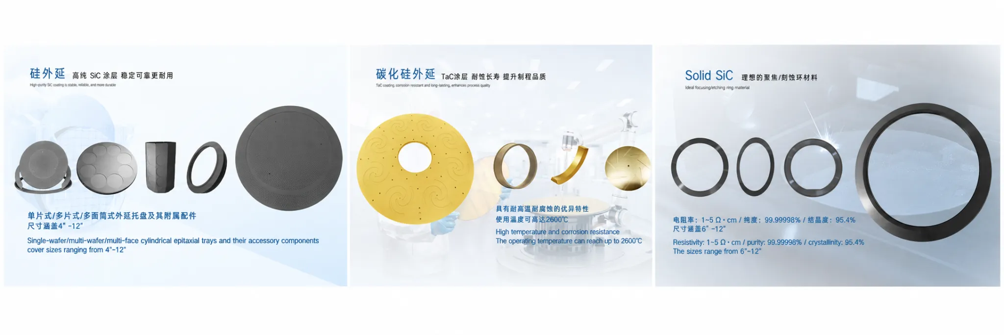
Figure 1 – VeTek Main Product Showcase
Core Conclusion: VeTek supports 1:1 customization based on customer drawings or original spare parts, covering major platforms such as Aixtron G10, Veeco K465i, ASM Epsilon, etc. Standard products can be shipped quickly; custom parts typically take 3–6 weeks.
What many engineers worry about most is not “whether it can be made,” but “whether it can be as stable as original parts, with controllable lead time, and complete inspection reports available.” One of VeTek’s core capabilities is full customization according to drawings while remaining compatible with major equipment brands.
The table below can be used directly for internal technical review or procurement evaluation:
|
Equipment Brand |
Typical Model |
Replaceable Parts |
Substrate Option |
Coating Option |
Ref. Lifetime |
|
Aixtron |
G10 |
Susceptor, Preheat Ring |
High-purity graphite |
SiC |
500–1000 h |
|
Veeco |
K465i |
Susceptor, Diversion Ring |
High-purity graphite |
SiC/TaC |
300–800 h |
|
ASM |
Epsilon series |
Susceptor, Focus Ring |
Solid SiC |
No coating |
2000+ h |
|
AMEC |
Etcher |
Focus Ring, Halfmoon |
Solid SiC/Graphite |
SiC |
By process |
In actual projects, we often receive original spare parts or CMM drawings from customers. The technical team will, after confirming thermal field matching and dimensional tolerances, provide recommendations on substrate purity, coating thickness and surface roughness, and supply samples for customer on-tool verification.
Core Conclusion: Thickness uniformity controlled within ±5%, density close to theoretical value, and controllable surface roughness are the core to suppressing powder shedding and particle contamination. Purity target is below 5 ppm, with critical metal impurities tracked by GDMS/ICP-OES.
Particle issues are almost the nightmare of every epitaxy engineer. Once the coating has local thin spots, pores or micro-cracks, powder will shed under repeated thermal cycling and corrosive gas attack, directly elevating wafer defect density.
Typical CVD SiC coating thickness is 100–200 μm. Through process parameter and flow field control, VeTek stabilizes thickness uniformity within ±5%. After more than 1000 thermal shock cycles (room temperature ↔ 1100°C), the coating shows no delamination and can meet the stringent GaN MOCVD requirement of particle defects ≤0.1/cm².
Overall purity of coating and components can be lower than 5 ppm, with some products reaching 99.99995%. We use ICP-OES and GDMS for trace metal analysis to ensure critical impurities such as Fe and Ni remain at controllable levels, avoiding interference with epitaxial layer doping or carrier concentration.
The β-SiC polycrystalline layer formed by the CVD process has density close to the theoretical value (approx. 3.21 g/cm³) with extremely low porosity. Surface roughness (Ra) can be adjusted according to customer process requirements, ensuring sufficient mechanical interlocking while avoiding becoming a particle generation source.
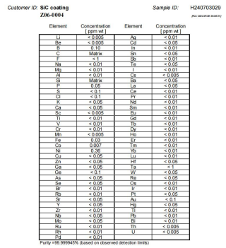
Figure 2 – GDMS Inspection Report for CVD SiC Coating
Core Conclusion: By precisely controlling the initial deposition rate and flow field to eliminate micro-stress, VeTek improved the coating yield of a customer’s MOCVD graphite susceptor from about 50% to 90%, and significantly extended service life.
This is a real story that happened on the production line. The customer reported edge yellowing and tendency to peel on some graphite susceptors, causing the overall coating yield of the batch to hover around 50% for a long time, with high line maintenance costs and wafer risk.
After the technical team led by Dr. Xiao intervened, two directions were focused on: first, the deposition rate in the initial stage was too fast, causing internal stress accumulation in the coating; second, flow field differences between the edge and center regions led to local over-thickness or under-thickness. By optimizing the MTS/H₂ ratio, deposition temperature profile and fixture flow field design, micro-stress was effectively released. Ultimately, the coating yield of that batch and subsequent production stabilized above 90%, the customer's replacement cycle was clearly extended, and particle complaints dropped significantly.
This case demonstrates: “being able to coat” is only the starting point; “coating stably, lasting long, and controlling particles” is the real value engineers care about. Data speaks louder than any promotion.
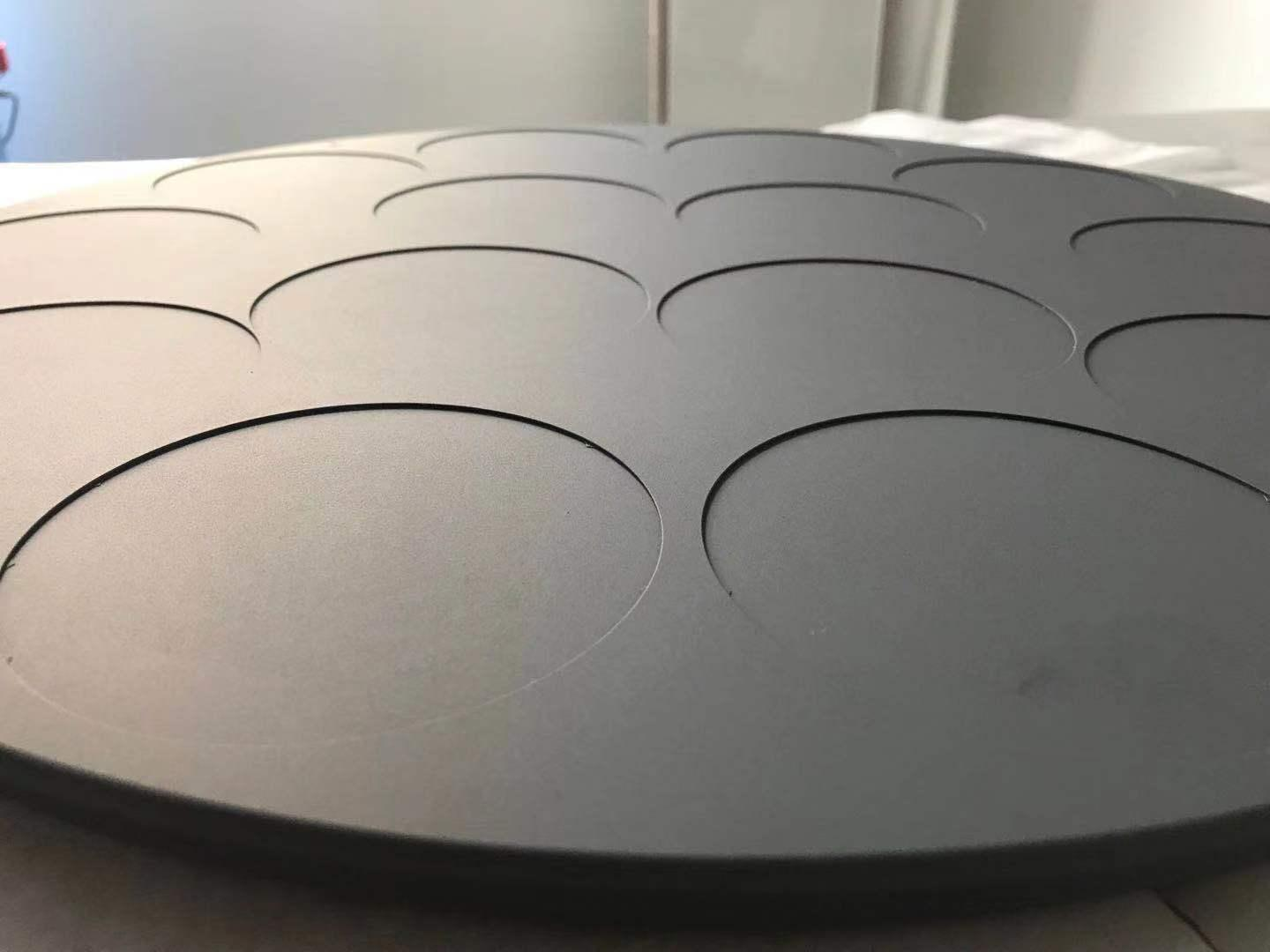
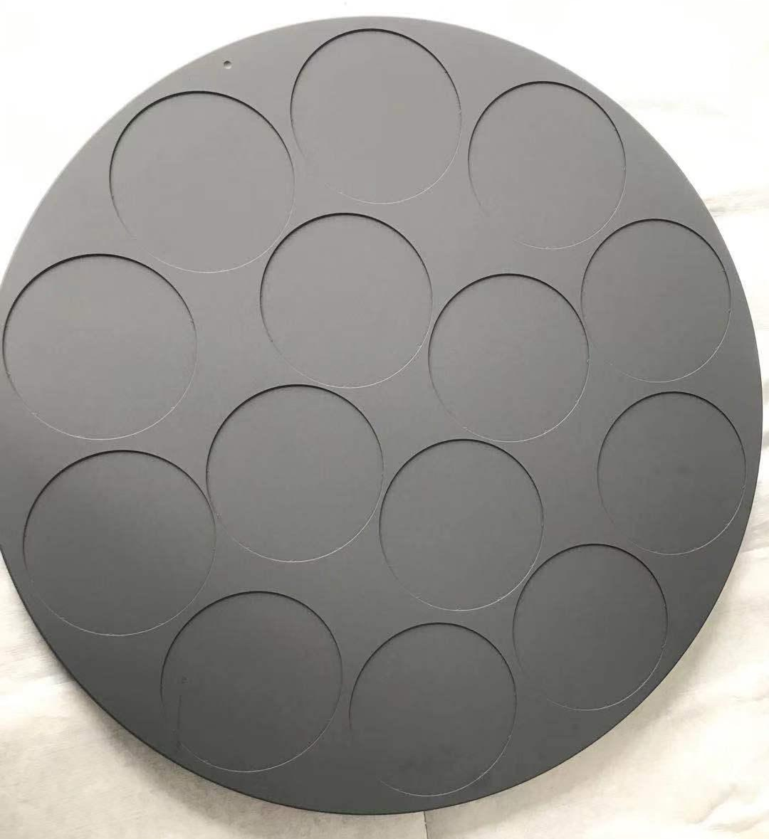
Figure 3 – High-Purity CVD Silicon Carbide Coated Graphite Susceptor with Uniform Surface Color and No Defects
Core Conclusion: Coated graphite parts have lower cost and faster thermal response, suitable for most epitaxy susceptors; Solid SiC has no interface risk and stronger plasma resistance, suitable for high-requirement etching components and ultra-long lifetime scenarios.
Many selection meetings struggle with: should we use coated graphite or go directly to Solid SiC? The two are not simply about “which is better,” but a trade-off between application scenario and total cost of ownership (TCO).
Advantages of coated graphite parts: High substrate thermal conductivity, fast heat-up, controllable cost; the coating provides chemical barrier and particle suppression. Suitable for large-size GaN/SiC epitaxy susceptors requiring high thermal uniformity.
Advantages of Solid SiC: Monolithic β-SiC with no coating-substrate interface, no delamination risk; purity can reach 5N–7N, outstanding resistance to plasma erosion, suitable for critical etching parts such as focus rings and showerheads, with lifetime up to 2000+ hours.
Core Conclusion: From installation monitoring and anomaly warning to professional cleaning & regeneration, forming a closed-loop management can significantly reduce TCO and decrease the frequency of new part procurement. VeTek provides dedicated cleaning services for Aixtron/Veeco and other equipment.
Many factories treat coated parts as “use-and-discard” consumables. In reality, after professional cleaning and regeneration, a considerable portion of components can be restored to particle levels and thermal performance close to new parts, especially susceptors and preheat rings for Aixtron and Veeco platforms.
It is recommended to establish a simple lifecycle log: record installation time, cumulative operating hours, surface condition after each cleaning, and particle test results. Only when the coating shows obvious yellowing, local delamination, or persistent particle exceedance should the replacement decision be triggered, rather than scrapping prematurely based on feeling.
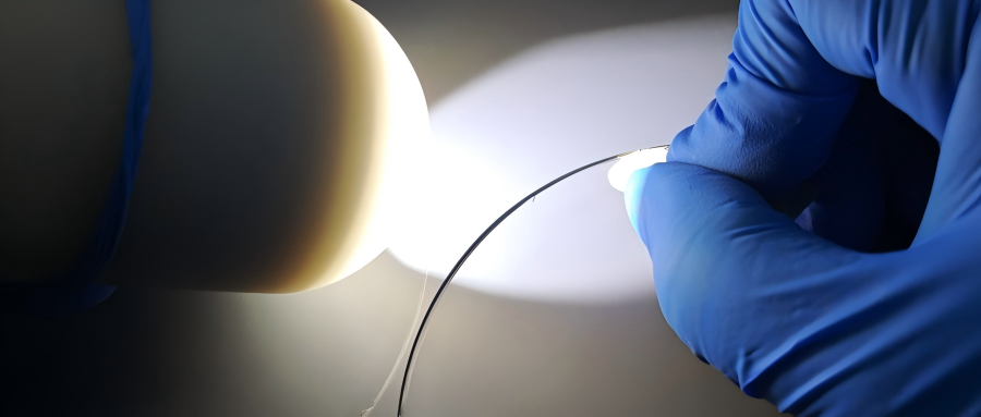
Figure 4 – CVD SiC Coating Graphite Parts Cleaning Service
Core Conclusion: Focus on ISO9001 system, complete inspection reports (GDMS/ICP-OES), sample support, lead-time reliability, and English technical communication capability. VeTek has 24/7 support and overseas customer service experience.
For international customers or factories with strict supplier qualification requirements, the following points are especially critical:
• Quality system: ISO9001, process controlled and traceable.
• Inspection capability: Provide complete material analysis reports for coating and substrate.
• Samples and lead time: Support sample evaluation; standard products ship quickly, custom parts typically 3–6 weeks, urgent orders can be expedited upon negotiation.
• Technical communication: Both sales and engineering teams can communicate fluently in English, reducing communication cost for overseas customers.
• After-sales response: Provide technical support and failure analysis assistance when coating or components show anomalies.
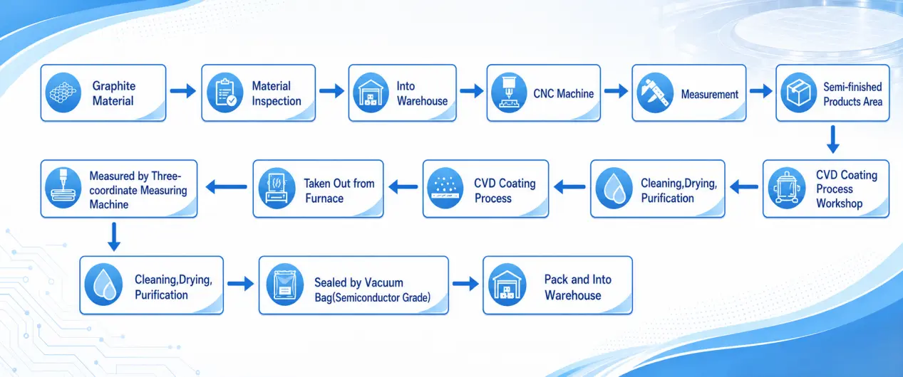
Figure 5 – VeTek Product Order Full Process
(1). Does the product support full customization based on drawings? Which major equipment can it match?
Yes. Can customize susceptor, preheat ring, diversion ring, halfmoon, focus ring, etc., compatible with platforms such as Aixtron G10, Veeco, ASM, AMEC, TEL.
(2). How is purity guaranteed? At what level are metal impurities controlled?
Coating and component purity can be lower than 5 ppm, some reaching 99.99995%. ICP-OES, GDMS and other equipment are used for trace analysis, with complete reports provided.
(3). What about thickness uniformity and service life of CVD SiC/TaC coatings?
Thickness uniformity is typically controlled within ±5%, thickness 100–200 μm. Under appropriate process windows, GaN MOCVD susceptor lifetime can reach the 500–1000 hour range; ultra-high-temperature scenarios require switching to TaC or Solid SiC.
(4). Is sample testing supported? What is the typical lead time for bulk orders?
Sample evaluation is supported. Standard products can be shipped quickly; custom parts typically take 3–6 weeks, depending on design complexity and volume. Urgent orders can be expedited upon negotiation.
(5). What quality system certifications are available? Can inspection reports and after-sales support be provided?
ISO9001 quality management system is in place. Material and coating analysis reports can be provided, along with 24/7 online technical support. English communication for overseas customers is seamless.
Selection is never about “choosing the most expensive” or “choosing the thickest,” but about “finding the solution with the best balance of performance and cost under your equipment, process window and particle budget.” We hope this handbook helps you quickly establish a decision framework: first look at temperature and atmosphere, then match the coating or Solid SiC, and finally validate lifetime and particle performance with data.
If you are evaluating replacement solutions for susceptors, preheat rings or hot-zone components on Aixtron, Veeco or other platforms, you are welcome to contact the VeTek technical team directly. We can provide customization recommendations, sample support and complete inspection reports based on your drawings or existing spare parts. Dr. Xiao and the engineering team are ready to discuss thermal field optimization or special structure development needs with you at any time.
For product details and more technical information, please contact us.
1. VeTek Semiconductor internal engineering data — SiC-coated graphite susceptor lifetime of 500–1000 hours under GaN MOCVD process, coating yield improved from 50% to 90% after resolving edge yellowing, and other practical cases [1].
2. T/CASME 2000-2025 Technical Specification for Silicon Carbide Coated Graphite Susceptors for Semiconductor Epitaxy — Specifies technical requirements for SiC-coated graphite susceptors prepared by CVD process on high-purity isostatic graphite substrates, applicable to semiconductor epitaxy products.
3. T/CASME 2085-2025 Technical Specification for Tantalum Carbide Coated Products for Silicon Carbide Crystal Growth — Technical specification for TaC-coated graphite products in SiC crystal growth scenarios.
4. Nakamura et al., “Sintered tantalum carbide coatings on graphite substrates: Highly reliable protective coatings for bulk and epitaxial growth,” Applied Physics Letters, Vol. 106, 082108, 2015. — Confirms that TaC coatings can effectively protect graphite substrates under high temperature (>2000°C) and strongly corrosive atmospheres, forming a clear performance boundary with SiC coatings.
5. Wang et al., “The effects of carbonized buffer layer on the growth of SiC on Si,” Journal of Crystal Growth, Vol. 199, pp. 564–567, 1999. — Discusses buffer layer effects and surface morphology control in SiC CVD growth process, indexed by Scopus and Web of Science.
Note: Lifetime and performance data in the text are typical reference values. Actual performance is affected by specific process conditions, equipment status and maintenance level. Please verify with actual measurements.
Author: VeTek Semiconductor Technical Engineering Team (completed under the guidance of Dr. Xiao)
For further technical discussion or sample evaluation, please contact us via the official website.
+86-579-87223657
Wangda Road, Ziyang Street, Wuyi County, Jinhua City, Zhejiang Province, China