


QR Code

Products
Contact Us


Fax
+86-579-87223657

Email

Address
Wangda Road, Ziyang Street, Wuyi County, Jinhua City, Zhejiang Province, China


|
Industry |
Power semiconductors, high-performance/AI packaging, optoelectronics and RF thermal management |
|
Process |
IGBT/SiC MOSFET module heat-spreading substrates, AI accelerator heat sinks/cold plates, laser and RF PA heat sinks |
|
Solution |
Selection and performance boundaries of diamond-copper, diamond-aluminum and diamond-SiC composites |
|
Services |
Material selection consulting, volume-fraction and CTE matching assessment, sample verification and application support |
|
Results |
• Comparable selection across three systems on k, CTE and density • Clear matching logic for power packaging and AI heat sinks • Volume fraction and interface set the performance ceiling • Checkable verification list before introduction |
The thermal bottleneck of high-power chips and modules is often not only “is conductivity high enough,” but whether conductivity and thermal expansion are matched together. Diamond composites raise thermal conductivity and lower CTE via high diamond volume fraction, forming three common paths: diamond-copper, diamond-aluminum and diamond-SiC. Based on typical performance ranges, this article explains selection boundaries, application scenarios and introduction checkpoints.
Core Conclusion: First set the thermal-conductivity target and the CTE matching object, then density and mechanical constraints. Diamond-copper has a higher conductivity ceiling and higher density; diamond-aluminum is strong on lightweighting; diamond-SiC has CTE closer to silicon, lower interface thermal resistance and good corrosion resistance—suited to strict matching and reliability needs.
All three can trade conductivity against CTE by adjusting diamond volume fraction (commonly about 30–70 vol%, typically 40–60%); relative density is usually required above 95%, and high density helps cut pore thermal resistance.
|
Dimension |
Diamond-Cu |
Diamond-Al |
Diamond-SiC |
|
k @ RT W/(m·K) |
500–900 (typ. 600–800) |
450–700 (typ. 450–600) |
300–800 (typ. 400–700) |
|
CTE ppm/K |
4–12 (typ. 6–9) |
4–12 (typ. 4–8) |
1–5 (typ. 2.0–3.5) |
|
Density g/cm³ |
5.2–7.3 (typ. 6.0–6.7) |
2.9–3.3 (typ. 3.0–3.2) |
2.9–3.4 (typ. 3.0–3.2) |
|
Flexural strength MPa |
100–400 (typ. 150–350) |
100–400 (typ. 200–300) |
300–540 (typ. 350–420) |
|
Better suited to |
Ultra-high-k power substrates |
Lightweight packaging, avionics |
Si-matched sinks, liquid cooling, high reliability |
Note: Ranges above are common engineering intervals and typical references; interface structure, diamond quality and density strongly affect the upper bound.
• Diamond-copper: Prefer when chasing a higher conductivity ceiling; density is higher than Al- and SiC-based systems—trade off for weight-sensitive designs.
• Diamond-aluminum: Clear lightweight advantage (about 3.0–3.2 g/cm³ class); suited to aerospace, portable and weight-limited packaging.
• Diamond-SiC: CTE can be tuned to about 2.0–3.5 ppm/K, closely matching silicon (about 2.5–2.6 ppm/K); a SiC reaction layer can form on diamond, lowering interface thermal resistance; corrosion-resistant and suited to liquid-cooling media and designs sensitive to warpage/shear stress.
Core Conclusion: Thermal conductivity decides “can heat leave quickly”; CTE matching decides “will thermal cycling tear the chip or solder.” Stacking conductivity alone without controlling mismatch often lowers junction temperature short term and hurts reliability long term.
AMB/DBC substrates for power modules (IGBT/SiC MOSFET), AI accelerator lids and cold plates, semiconductor laser heat sinks, and 5G/6G PA and radar T/R components all face high heat flux and repeated thermal cycling. Raising diamond volume fraction can lower overall CTE and raise conductivity potential; interface bond quality then sets interface thermal resistance and thermal-shock behavior.
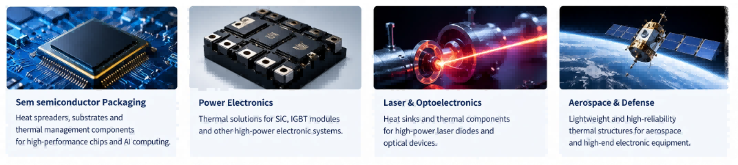
• Power semiconductor packaging: Lower junction temperature, raise power density and reliability (EV inverters, industrial drives, rail, etc.).
• High-performance/AI servers: GPU/TPU heat sinks and liquid cold plates to cut chip temperature under high heat flux.
• Optoelectronics/lasers: LD, disk laser and VCSEL heat sinks needing both conductivity and dimensional stability.
• RF/microwave and aerospace: High-power amplifiers and airborne/missile components needing high k, low CTE and low mass.
• Precision instruments/optics: High specific stiffness, hardness and wear resistance for chucks, scan mirrors and similar stable structures.
Core Conclusion: Do not rely on nominal thermal conductivity alone. Check diamond volume fraction and density, CTE match to chip/substrate, interface condition, mechanical strength and machinability, then close with small-batch thermal cycling and thermal-resistance tests.
Recommended verification sequence:
1. Duty: heat flux, max temperature, medium (air/liquid cooling), CTE target vs chip or ceramic substrate.
2. Material: volume fraction, density, room-temperature k, CTE, flexural strength; for diamond-SiC also reaction layer and corrosion resistance.
3. Structure: dimensional tolerance, surface condition, compatibility with solder/sinter/mechanical assembly.
4. Validation: small-batch thermal resistance, thermal cycling (watch delamination and resistance drift), and same-condition comparison with existing copper/ceramic solutions when needed.
Core Conclusion: When failure shows up as solder fatigue or substrate warpage after thermal cycling—not only high steady-state junction temperature—stacking more copper conductivity often treats symptoms. Moving to a diamond composite with CTE closer to the chip/ceramic attacks the mismatch root cause.
Engineering Note:
An automotive power-module line, after raising current density, could still hold steady-state junction temperature with stronger water cooling, but accelerated thermal cycling produced earlier solder cracks and local thermal-resistance climb. Failure analysis showed shear stress accumulating from substrate–chip CTE difference under cycling, not a single hot-spot cooling shortfall. The team then evaluated diamond-copper and diamond-SiC samples at the same package size: the former offered higher k, the latter CTE closer to silicon and ceramic substrates. Small-batch comparison showed that, at similar thermal-resistance targets, the better-matched CTE option had smaller resistance drift after cycling and later crack initiation. The decision point was not “diamond composites always conduct best,” but that the failure mode already pointed to mismatch; writing volume fraction, interface and CTE into the specification is more actionable than only “k ≥ XX.” This case shows: the value of diamond composites is the combination of conductivity and matching—not a single-metric contest.
1. Is higher diamond volume fraction always better?
No. Higher volume fraction usually raises conductivity potential and lowers CTE, but also increases machining difficulty, densification challenge and cost. Balance target k, CTE, strength and manufacturability; a common engineering window is about 40–60 vol%.
2. Is diamond-SiC always better than diamond-copper?
It depends on constraints. When ultra-high conductivity is needed and higher density is acceptable, diamond-copper is often more competitive; when close silicon match, lightweighting or liquid-cooling corrosion resistance matters, diamond-SiC more often makes the short list.
3. Can nominal thermal conductivity be used directly in thermal design?
Treat it as a screening range; design to measured thermal resistance and plant process windows. Interface resistance, porosity and anisotropy can separate “material k” from “system thermal resistance.”
4. How do these work with AlN or alumina ceramic substrates?
Ceramic substrates emphasize insulation and structure; diamond composites emphasize high in-plane/through-plane conductivity and CTE tuning. They often work in layers within a module; align CTE and interface process in selection. Cross-read with advanced ceramics selection content.
5. What should a minimum verification set include?
Volume fraction and density, k and CTE, critical dimensions and surface, thermal resistance, post-cycling delamination/resistance drift. For liquid cooling, add medium compatibility and corrosion-related checks.
Diamond composites are not simply “higher-k copper/aluminum substitutes,” but a path that co-tunes conductivity and CTE via diamond volume fraction and interface engineering. Diamond-copper, diamond-aluminum and diamond-SiC each have boundaries in density, matching and environmental resistance; lock the failure mode and matching object first, then choose system and volume fraction, and validate with small-batch thermal resistance and cycling—more reliable than comparing nominal k alone.
If you need material assessment for power-module substrates, AI heat sinks or laser/RF heat sinks, you are welcome to contact the VeTek technical team. Dr. Xiao and the engineering team can assist with performance-range comparison, sample verification and application discussion.
Main References and Data Sources
1. Diamond composite performance parameter table (diamond-copper / aluminum / SiC: volume fraction, density, thermal conductivity, CTE, strength and application scenarios).
2. VeTek Semiconductor thermal management and advanced materials engineering practice notes.
3. VeTek official website: https://www.veteksemicon.com/ and other-semiconductor-ceramics related pages.
Note: Performance ranges in the text are typical engineering references and depend strongly on diamond quality, interface process and density; actual values follow measurement and plant verification.
Author: VeTek Semiconductor Technical Engineering Team (completed under the guidance of Dr. Xiao)
For further technical discussion or sample evaluation, please contact us via the official website.
+86-579-87223657
Wangda Road, Ziyang Street, Wuyi County, Jinhua City, Zhejiang Province, China