


QR Code

Products
Contact Us


Fax
+86-579-87223657

E-mail

Address
Wangda Road, Ziyang Street, Wuyi County, Jinhua City, Zhejiang Province, China


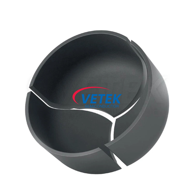
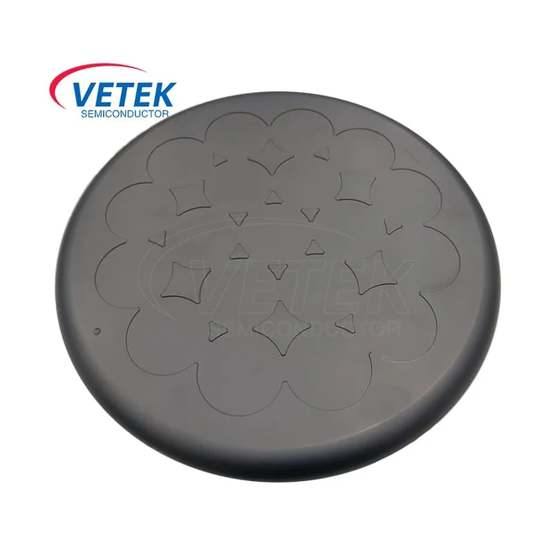
We are going to dedicate ourselves to providing our esteemed buyers together with the most enthusiastically thoughtful products and services for Silicon-base GaN epitaxy, SiC epitaxy, Monocrystalline silicon epitaxy, Deep UV epitaxy, semiconductor etching, We now have substantial goods source and also the rate is our advantage. Welcome to inquire about our merchandise.
Silicon-base GaN epitaxy, For many years, we now have adhered to the principle of customer oriented, quality based, excellence pursuing, mutual benefit sharing. We hope, with great sincerity and good will, to have the honor to help with your further market.


+86-579-87223657
Wangda Road, Ziyang Street, Wuyi County, Jinhua City, Zhejiang Province, China