


")
 Coating (2/2) - VeTek Semiconductor")


QR Code

Products
Contact Us


Fax
+86-579-87223657

E-mail

Address
Wangda Road, Ziyang Street, Wuyi County, Jinhua City, Zhejiang Province, China


VeTek Semiconductor is manufacturer committed to providing high quality CVD TaC Coating and CVD SiC Coating Collector Bottom and work closely with Aixtron equipment to meet the needs of our customers. Whether in process optimization or new product development, we are ready to provide you with technical support and answer any questions you may have.
Process stability guarantee
Temperature gradient control: ±1.5℃/cm@1200℃
Flow field optimization: The special channel design makes the reaction gas distribution uniformity up to 92.6%
Equipment protection mechanism
Dual protection:
Thermal shock buffer: withstand 10℃/s rapid temperature change
Particle interception: Trapping > 0.3μm sediment particles
|
Direction of application |
Specific process parameters |
Customer value |
|
Grade IGBT |
10^17/cm³ doping uniformity |
Yield increased by 8-12% |
|
5G RF device |
Surface roughness < 0.15nm Ra |
Carrier mobility increased by 15% |
| PV HJT equipment |
Anti-PID aging test > 3000 cycles |
Equipment maintenance cycle extended to 9000 hours |
Production traceability system
Source of raw materials: Tokai/Toyo Graphite from Japan,SGL graphite from Germany
Digital twin monitoring: Each component is matched to an independent process parameter database
Third generation semiconductor manufacturing
Scenario: 6-inch SiC epitaxial growth (100-150μm thickness control)
Compatible model: Aixtron G5 WW/CRIUS II
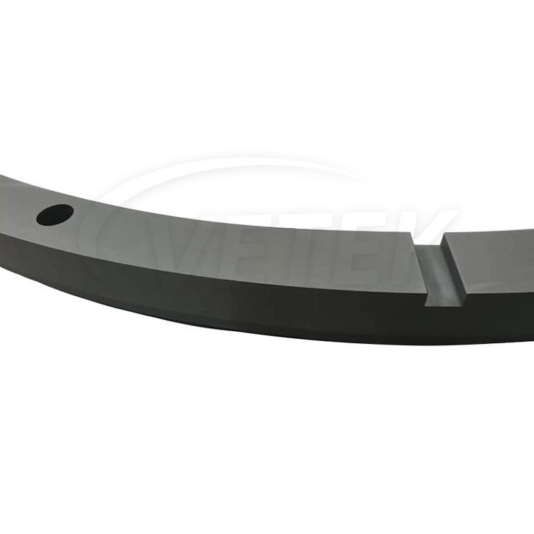
By using Aixtron SiC coated Collector Top, Collector Center and SiC Coated Collector, thermal management and chemical protection in semiconductor manufacturing processes can be achieved, the film growth environment can be optimized, and the quality and consistency of the film can be improved. The combination of these components in Aixtron equipment ensures stable process conditions and efficient semiconductor production.

| Basic physical properties of CVD SiC coating | |
| Property | Typical Value |
| Crystal Structure | FCC β phase polycrystalline, mainly (111) oriented |
| Density | 3.21 g/cm³ |
| Hardness | 2500 Vickers hardness(500g load) |
| Grain SiZe | 2~10μm |
| Chemical Purity | 99.99995% |
| Heat Capacity | 640 J·kg-1·K-1 |
| Sublimation Temperature | 2700℃ |
| Flexural Strength | 415 MPa RT 4-point |
| Young' s Modulus | 430 Gpa 4pt bend, 1300℃ |
| Thermal Conductivity | 300W·m-1·K-1 |
| Thermal Expansion(CTE) | 4.5×10⁻⁶K-1 |


Address
Wangda Road, Ziyang Street, Wuyi County, Jinhua City, Zhejiang Province, China
Tel
+86-579-87223657
Wangda Road, Ziyang Street, Wuyi County, Jinhua City, Zhejiang Province, China