Products

China Semiconductor wafer processing processes Manufacturer, Supplier, Factory

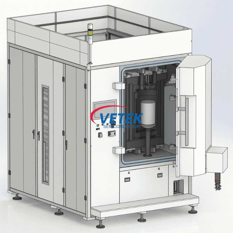
Our organization sticks for the principle of "Quality will be the life of your business, and name may be the soul of it" for Semiconductor wafer processing processes, High Purity Quartz Wafer Boat, Wafer used quartz boat market, Quartz wafer boat, Quartz boat wafer, Leading the trend of this field is our persistent objective. Supplying first class solutions is our intention. To create a beautiful upcoming, we wish to cooperate with all close friends in the home and overseas. Should you have got any interest in our products and solutions, remember to never wait to call us.
Semiconductor wafer processing processes, We have been your reliable partner in international markets with the best quality items. Our advantages are innovation, flexibility and reliability which have been built during the last twenty years. We focus on providing service for our clients as a key element in strengthening our long-term relationships. Our continual availability of high grade products in combination with our excellent pre-sales and after-sales service ensures strong competitiveness in an increasingly globalized market.

Hot Products

  • EDM graphite electrode

    EDM graphite electrode

    EDM graphite electrode has the characteristics of moderate density, smooth surface and low cost, and is suitable for chemical industry, metal smelting, etc. VeTek Semiconductor has strong production capacity and rich export experience in EDM graphite electrode products. You are welcome to inquire at any time.
  • Ceramic Electrostatic Chuck

    Ceramic Electrostatic Chuck

    Ceramic Electrostatic Chuck is widely used in semiconductor manufacturing and processing to fix wafers. It is an indispensable tool for high-precision wafer processing. VeTek Semiconductor is an experienced manufacturer and supplier of Ceramic Electrostatic Chuck, and can provide highly customized products according to different customer needs.
  • SiC Coating Cover Segments Inner

    SiC Coating Cover Segments Inner

    At VeTek Semiconductor, we specialize in the research, development, and industrialization of CVD SiC coating and CVD TaC coating. One exemplary product is the SiC Coating Cover Segments Inner, which undergoes extensive processing to achieve a highly precise and densely coated CVD SiC surface. This coating demonstrates exceptional resistance to high temperatures and provides robust corrosion protection. Feel free to contact us for any inquiries.
  • Silicon Pedestal

    Silicon Pedestal

    VeTek Semiconductor Silicon Pedestal is a key component in semiconductor diffusion and oxidation processes. As a dedicated platform for carrying silicon boats in high-temperature furnaces, the Silicon Pedestal has many unique advantages, including improved temperature uniformity, optimized wafer quality, and enhanced performance of semiconductor devices. For more product information, please feel free to contact us.
  • MOCVD Susceptor with TaC Coating

    MOCVD Susceptor with TaC Coating

    VeTek Semiconductor is a comprehensive supplier involved in the research, development, production, design, and sales of TaC coatings and SiC coating parts. Our expertise lies in the production of state-of-the-art MOCVD Susceptor with TaC Coating, which play a vital role in the LED epitaxy process. We welcome you to discuss with us inquiries and further information.
  • Focus ring for Etching

    Focus ring for Etching

    Focus ring for Etching is the key component to ensure process accuracy and stability. These components are precisely assembled in a vacuum chamber to achieve uniform machining of nanoscale structures on the wafer surface through precise control of plasma distribution, edge temperature and electric field uniformity.

Send Inquiry

X
We use cookies to offer you a better browsing experience, analyze site traffic and personalize content. By using this site, you agree to our use of cookies. Privacy Policy
Reject Accept