
QR Code
Products
Contact Us


Fax
+86-579-87223657

Email

Address
Wangda Road, Ziyang Street, Wuyi County, Jinhua City, Zhejiang Province, China
|
Industry |
Semiconductor manufacturing (chamber structural, insulating, thermal and plasma-exposed parts) |
|
Process |
Etch, deposition, diffusion/anneal and related hot-zone, insulation and wear-part selection |
|
Solution |
Four-dimension selection framework and duty boundaries for Al₂O₃ / AlN / Si₃N₄ / bulk SiC |
|
Services |
Material selection consulting, drawing-based customization, sample verification, boundary vs coating solutions |
|
Results |
• Actionable temperature–corrosion–electrical–mechanical decision sequence • Clear role split among four materials; fewer mix-ups • Bulk SiC not confused with CVD coating path • Drill-down to Si₃N₄ topic and pillar overview |
When a chamber ceramic part fails and alumina, aluminum nitride, silicon nitride and bulk silicon carbide are all on the table, the real question is: under the current temperature, corrosive medium, electrical and mechanical constraints, which material can control lifetime, particles and cost together. This article gives a four-dimension assessment framework and a four-material comparison, and draws a clear line between bulk SiC and graphite CVD coating.
Core Conclusion: Do not start with unit price or “sounds more advanced.” First lock the temperature window and corrosive medium, then whether high insulation / high thermal conductivity / low CTE is required, and finally close with mechanical impact, machining cost and design constraints. Selection is reusable only when all four dimensions land on checkable process descriptions.
Recommended decision sequence:
1. Temperature: Does long-term duty sit in alumina's comfort zone, enter AlN's thermal-conductivity advantage band, or need Si₃N₄ / SiC margins for high temperature and thermal shock?
2. Corrosion / plasma: Under fluorine- or chlorine-containing plasma or specific chemistries, when etch rates differ by an order of magnitude, material choice is often already locked. Alumina loss in fluorine plasma is typically much higher than bulk SiC.
3. Electrical: Is high insulation mandatory? Is low CTE matched to silicon plus higher thermal conductivity needed (AlN often discussed for chucks / thermal structures)?
4. Mechanical: Impact, clamp preload, wall thickness and sharp corners—many early ceramic failures are design stress concentration, not wrong grade. Si₃N₄ often beats ordinary alumina on strength–toughness combination.
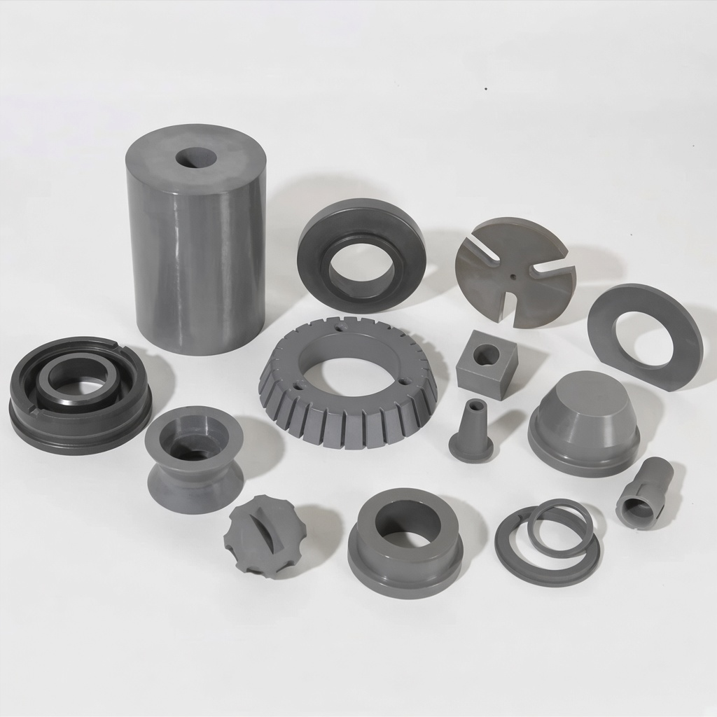
Core Conclusion: Prefer alumina for mid/low-temperature insulation and cost; evaluate AlN when high thermal conductivity and silicon match matter; look at Si₃N₄ for high strength and thermal-shock margin; evaluate bulk SiC for strong-plasma wear and ultra-clean critical positions.
|
Dimension |
Al₂O₃ |
AlN |
Si₃N₄ |
Bulk SiC |
|
Temp. comfort |
Mid/low T, cost-effective |
Mid/high T, k advantage |
High T + shock margin |
High T / plasma wear |
|
Thermal conductivity |
Moderate–low |
High (chuck/thermal) |
Moderate (structural grade) |
High, process/density dependent |
|
Strength / toughness |
Common insulation structure |
High sinter/machine cost |
High strength + good toughness |
Wear and etch resistance strong |
|
Plasma exposure |
Faster loss in F plasma |
Process-dependent, not wear first choice |
Structural / some chamber parts |
Often chosen for focus rings etc. |
|
Typical parts |
Insulators, spacers, structure |
ESC, thermal structures |
Fixtures, AMB substrates, shafts/rings |
Focus rings, high-purity wear parts |
Note: Table is a selection-logic summary, not a full materials handbook. Detailed Si₃N₄ parameters are in the silicon nitride topic; bulk SiC and graphite + CVD SiC coating are not the same technical path.
• About ≤400 °C: alumina is often the default insulation/structure option for cost and mature machining.
• About 400–800 °C with emphasis on thermal conductivity and silicon match: AlN enters evaluation (ESC, thermal structures, etc.), accepting higher sinter and machining cost.
• Higher temperature, rapid thermal cycling or strong mechanical impact: Si₃N₄ and bulk SiC more often make the short list; plasma-exposed wear positions preferentially consider bulk SiC.
Core Conclusion: Bulk SiC is the bulk material with no coating–substrate interface; graphite + CVD SiC is a coating deposited on graphite, focused on thickness uniformity, adhesion and particles. Search intent and failure modes differ—do not conflate them.
This cluster only discusses bulk ceramic parts. If your question is coating thickness, uniformity, cleaning/regeneration or particle control on epitaxial hot-zone graphite susceptors, go to the Graphite Parts CVD Silicon Carbide Coating Topic / CVD Coating Consumables Selection Engineering Handbook. For etch focus rings and similar positions, only when the failure mode is interface delamination does evaluating a bulk Solid SiC path become more appropriate.
Core Conclusion: When the lifetime bottleneck is plasma etch rate rather than insulation or thermal conductivity, thickening alumina or changing more often only delays the problem; reselecting by the corrosion dimension changes the cost curve.
Engineering Note:
An etch chamber edge ring originally used an alumina solution; under fluorine processes wear accelerated, replacement intervals shortened and downtime cost rose. The team first checked process window and fit-up tolerances and confirmed failure was dominated by surface etch thinning, not mechanical impact cracking. In the four-dimension frame: temperature and insulation remained acceptable; corrosion became the binding constraint. Bulk SiC samples were then compared at the same envelope; small-batch data showed clearly lower wear rate and longer replacement life. Unit price was higher, but total cost improved when downtime and throughput were included. Introduction emphasized that bulk SiC and “graphite coating rings” are not the same specification language—drawings, tolerances and thermal/electrical behavior must be verified separately. The case shows: selection should reverse from failure mode to constraint dimension, not from material reputation to justification.
1. Can one datasheet table decide the material?
No. Datasheets are screening tools; the final call comes from temperature, corrosion, electrical and mechanical dimensions plus plant verification. Grade, microstructure and machining state all shift the upper bound.
2. Is AlN always “better” than alumina?
AlN often has the edge when thermal conductivity and silicon match matter, but sinter densification and machining cost are higher. For mid/low-temperature pure insulation structures, alumina often remains a reasonable default.
3. Structural-grade Si₃N₄ has moderate thermal conductivity—can it still be a power substrate?
Structural grades emphasize mechanics and thermal shock; power AMB and similar needs must be evaluated against substrate-grade products and module thermal-resistance targets—see the silicon nitride topic.
4. How do quartz and these four ceramics share roles?
Quartz emphasizes high purity, optical/RF transmission and conventional high-temperature inert duty; ceramics cover wear resistance, high-strength insulation and strong plasma exposure. See the pillar page role split.
5. What should I read next?
Overall framework: pillar page. Si₃N₄ detail: silicon nitride selection article. Quartz purity and crystallization: C2. Coating questions: CVD coating cluster.
Alumina, AlN, Si₃N₄ and bulk SiC have no absolute ranking—only fit to current constraints. Narrow options with the temperature–corrosion–electrical–mechanical sequence, validate assumptions against the failure mode, then decide whether to change material or only design and maintenance. Keep bulk SiC questions in this cluster; send graphite coating questions to the coating topic.
If you need a four-material comparison or drawing-based assessment for a specific chamber part, you are welcome to contact the VeTek technical team. Dr. Xiao and the engineering team can assist with selection discussion and sample verification.
Product entry: https://www.veteksemicon.com/other-semiconductor-ceramics
Main References and Data Sources
1. Advanced Ceramics and Quartz Blog Cluster Plan (material comparison and four-dimension selection architecture).
2. VeTek Silicon Nitride and related product typical parameters and internal engineering practice.
3. Pillar page Selection Guide for Advanced Ceramic and Quartz Parts and existing CVD coating cluster boundary notes.
Note: Temperature bands and performance comparisons in the text are engineering-framework references; actual values follow grade, process conditions and plant verification.
Author: VeTek Semiconductor Technical Engineering Team (completed under the guidance of Dr. Xiao)
For further technical discussion or sample evaluation, please contact us via the official website.
+86-579-87223657
Wangda Road, Ziyang Street, Wuyi County, Jinhua City, Zhejiang Province, China
Copyright © 2024 WuYi TianYao New Material Tech.Co.,Ltd. All Rights Reserved.
Sitemap | RSS | XML | Privacy Policy |