Products

China Silicon Carbide Ceramic Wafer Boat supplier Manufacturer, Supplier, Factory

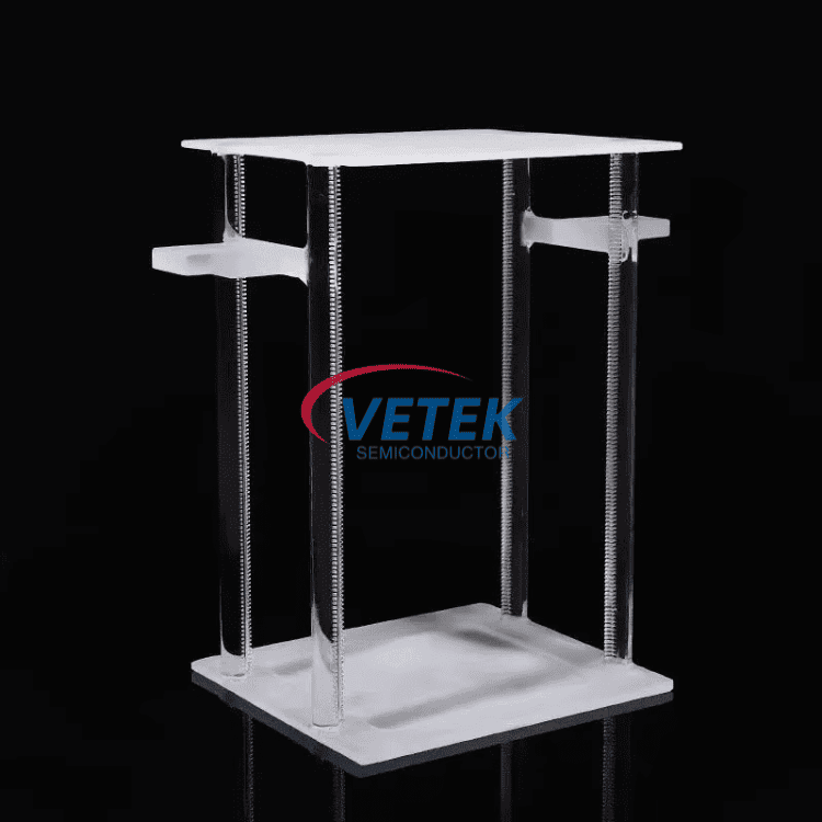
We rely upon strategic thinking, constant modernisation in all segments, technological advances and of course upon our employees that directly participate in our success for Silicon Carbide Ceramic Wafer Boat supplier, Silicon Carbide Ceramic Wafer Boat, wafer used quartz boat, quartz wafer boat, semiconductor wafer boat, If you're interested in any of our products and services, make sure you don't be reluctant to call us. We've been wanting to reply you within 24 several hours just after receipt of your respective ask for and to generate mutual un-limited positive aspects and enterprise in in the vicinity of long run.
Silicon Carbide Ceramic Wafer Boat supplier, Our expert engineering team will generally be prepared to serve you for consultation and feedback. We're able to also give you with free of charge samples to meet your requirements. Best efforts will likely be produced to provide you the best service and merchandise. When you are keen on our business and items, make sure you speak to us by sending us emails or call us quickly. In an effort to know our merchandise and company extra, you may come to our factory to view it. We'll generally welcome guests from all over the world to our business to create business relations with us. Be sure to feel cost-free to speak to us for small business and we believe we are going to share the best trading experience with all our merchants.

Hot Products

  • Tantalum Carbide Guide Ring

    Tantalum Carbide Guide Ring

    VeTek Semiconductor is a professional manufacturer and leader of Tantalum Carbide Guide Ring products in China. Our Tantalum Carbide (TaC) Guide Ring is a high-performance ring component made of tantalum carbide, which is commonly used in semiconductor processing equipment, especially in high-temperature and highly corrosive environments such as CVD, PVD, etching and diffusion. VeTek Semiconductor is committed to providing advanced technology and product solutions for the semiconductor industry, and welcomes your further inquiries.
  • CVD SiC Block for SiC Crystal Growth

    CVD SiC Block for SiC Crystal Growth

    CVD SiC Block for SiC Crystal Growth, is a new high purity raw material developed by Vetek Semiconductor. It has a high input-output ratio and can grow high-quality, large-size silicon carbide single crystals, which is a second-generation material to replace the powder used in the market today. Welcome to discuss technical issues.
  • TaC Coating Planetary Susceptor

    TaC Coating Planetary Susceptor

    TaC Coating Planetary Susceptor is an exceptional product for Aixtron epitaxy equipment. VeTek Semiconductor's TaC coating provides excellent high-temperature resistance and chemical inertness. This unique combination ensures reliable performance and long service life, even in demanding environments. VeTek is committed to providing high-quality products and serving as a long-term partner in the Chinese market with competitive pricing.
  • MOCVD Susceptor with TaC Coating

    MOCVD Susceptor with TaC Coating

    VeTek Semiconductor is a comprehensive supplier involved in the research, development, production, design, and sales of TaC coatings and SiC coating parts. Our expertise lies in the production of state-of-the-art MOCVD Susceptor with TaC Coating, which play a vital role in the LED epitaxy process. We welcome you to discuss with us inquiries and further information.
  • High Purity Porous Graphite

    High Purity Porous Graphite

    High Purity Porous Graphite provided by VeTek Semiconductor is an advanced semiconductor processing material. It is made of high-purity carbon material with excellent thermal conductivity, good chemical stability and excellent mechanical strength. This High Purity Porous Graphite plays an important role in the growth process of single crystal SiC. VeTek Semiconductor is committed to providing quality products at competitive prices and looks forward to becoming your long-term partner in China.Welcome to consult at any time.
  • Focus ring for Etching

    Focus ring for Etching

    Focus ring for Etching is the key component to ensure process accuracy and stability. These components are precisely assembled in a vacuum chamber to achieve uniform machining of nanoscale structures on the wafer surface through precise control of plasma distribution, edge temperature and electric field uniformity.

Send Inquiry

X
We use cookies to offer you a better browsing experience, analyze site traffic and personalize content. By using this site, you agree to our use of cookies. Privacy Policy
Reject Accept