Products

China Semiconductor Ceramic Nozzle Manufacturer, Supplier, Factory

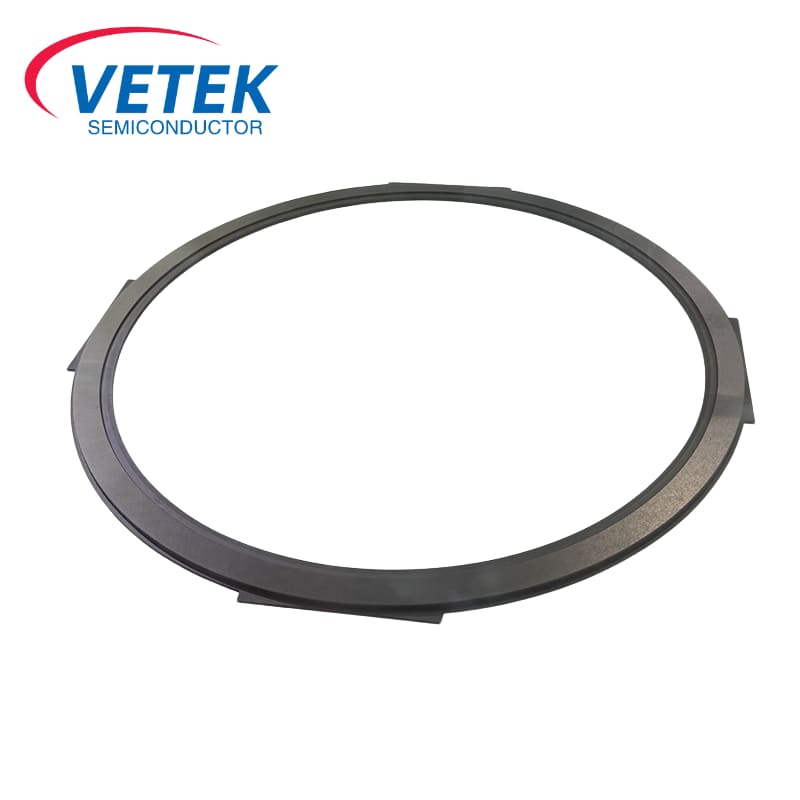
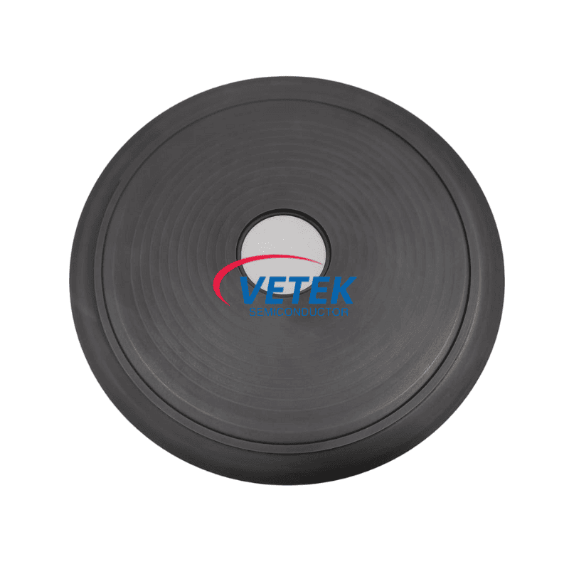
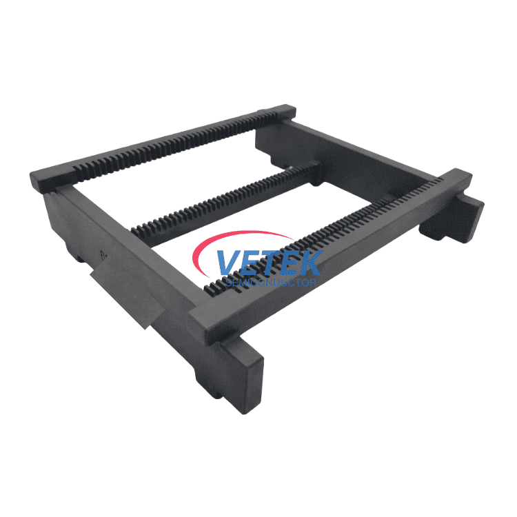
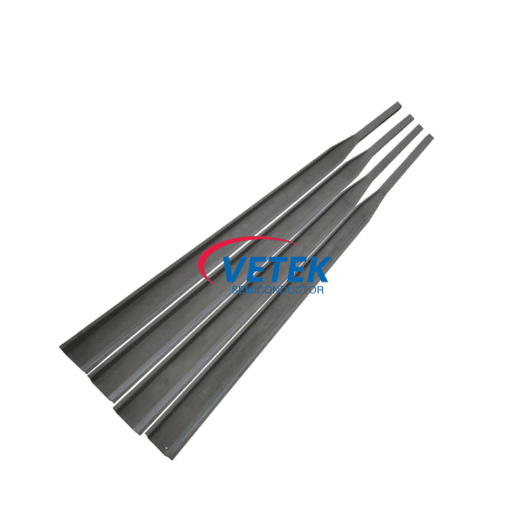
Our organization sticks for the principle of "Quality will be the life of your business, and name may be the soul of it" for Semiconductor Ceramic Nozzle, Ceramic Nozzle, semiconductor ceramics, ceramic nozzles for sandblasting, ceramic nozzle spray, Leading the trend of this field is our persistent objective. Supplying first class solutions is our intention. To create a beautiful upcoming, we wish to cooperate with all close friends in the home and overseas. Should you have got any interest in our products and solutions, remember to never wait to call us.
Semiconductor Ceramic Nozzle, Taking the core concept of "to be the Responsible". We will redound up on society for high quality solutions and good service. We are going to initiative to participate in international competition to be a first- class manufacturer of this product in the world.

Hot Products

  • SiC Shower Head

    SiC Shower Head

    VeTek Semiconductor is a leading SiC Shower Head manufacturer and innovator in China.We have been specialized in SiC material for many years.SiC Shower Head is chosen as a focusing ring material due to its excellent thermochemical stability, high mechanical strength and resistance to plasma erosion.We look forward to becoming your long-term partner in China.
  • Quartz Wafer Boat

    Quartz Wafer Boat

    Vetek Semiconductor Quartz Wafer Boat is designed to exceed industry standards and optimize your production process. Our quartz wafer boats are carefully designed and highly reliable to meet the stringent requirements of the semiconductor industry. We look forward to your consultation.
  • Semiconductor Quartz tank

    Semiconductor Quartz tank

    VeTek semiconductor is a leading semiconductor quartz tank manufacturer and factory in China. In fact, quartz tank is particularly important in the wet processing used in wafer manufacturing. Welcome your further inquiries.
  • SiC Block

    SiC Block

    Veteksemicon’s SiC Block is designed for high-efficiency grinding and thinning of silicon and sapphire wafers. With excellent thermal conductivity (≥120 W/m·K), high thermal shock resistance, and superior wear resistance (Mohs ≥9), our blocks improve process stability and reduce tool change frequency. Available in sizes from 120mm to 480mm, with customized options and fast delivery to meet diverse production needs.
  • Silicon On Insulator Wafer

    Silicon On Insulator Wafer

    VeTek Semiconductor is a professional Chinese manufacturer of Silicon On Insulator Wafer. the Silicon On Insulator Wafer is an important semiconductor substrate material, and its excellent product characteristics make it play a key role in high-performance, low-power, high-integration and RF applications. Looking forward to your consultation.
  • Physical Vapor Deposition

    Physical Vapor Deposition

    Vetek semiconductor Physical Vapor Deposition (PVD) is an advanced process technology widely used in surface treatment and thin film preparation. PVD technology uses physical methods to directly transform materials from solid or liquid to gas and form a thin film on the surface of the target substrate. This technology has the advantages of high precision, high uniformity and strong adhesion, and is widely used in semiconductors, optical devices, tool coatings and decorative coatings. Welcome to discuss with us!

Send Inquiry

X
We use cookies to offer you a better browsing experience, analyze site traffic and personalize content. By using this site, you agree to our use of cookies. Privacy Policy
Reject Accept