Products

China Ceramic Nozzle Manufacturer, Supplier, Factory

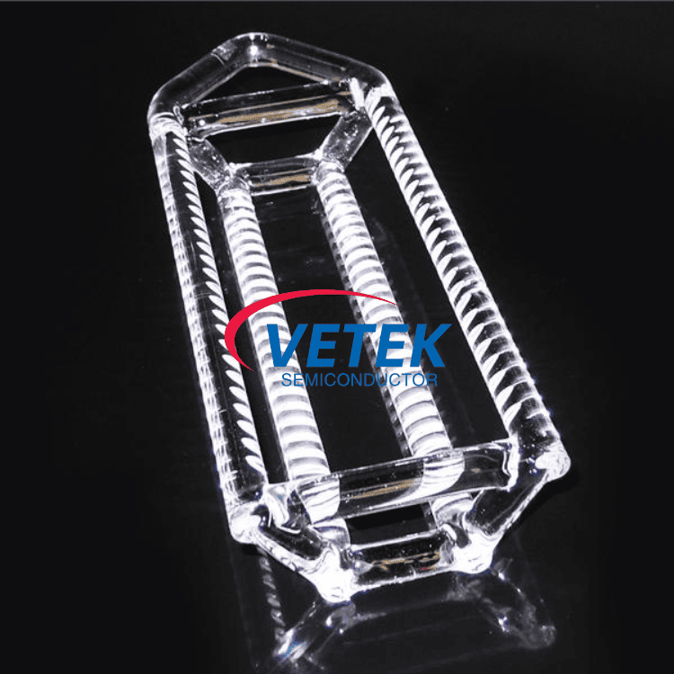
To be able to ideal meet up with client's needs, all of our operations are strictly performed in line with our motto "High High-quality, Competitive Cost, Fast Service" for Ceramic Nozzle, Semiconductor Ceramic Nozzle, semiconductor ceramics, ceramic nozzles for sandblasting, ceramic nozzle spray, We play a leading role in giving buyers with high-quality goods fantastic provider and competitive selling prices.
Ceramic Nozzle, Our company mission is that providing high quality and beautiful products with reasonable price and strive to gain 100% good reputation from our clients. We believe Profession achieves excellence! We welcome you to cooperate with us and grow up together.

Hot Products

  • Semiconductor thermal spraying technology

    Semiconductor thermal spraying technology

    Vetek Semiconductor Semiconductor thermal spraying technology is an advanced process that sprays materials in a molten or semi-molten state onto the surface of a substrate to form a coating. This technology is widely used in the field of semiconductor manufacturing, mainly used to create coatings with specific functions on the surface of the substrate, such as conductivity, insulation, corrosion resistance, and oxidation resistance. The main advantages of thermal spraying technology include high efficiency, controllable coating thickness, and good coating adhesion, making it particularly important in the semiconductor manufacturing process that requires high precision and reliability. Looking forward to your inquiry.
  • Silicon Carbide Wafer Boat

    Silicon Carbide Wafer Boat

    VeTek Semiconductor's high-purity Silicon Carbide Wafer Boat is made of extremely pure silicon carbide material with excellent thermal stability, mechanical strength and chemical resistance. High-purity Silicon Carbide Wafer Boat is used in hot zone applications in semiconductor manufacturing, especially in high-temperature environments, and plays an important role in protecting wafers, transporting materials and maintaining stable processes. VeTek Semiconductor will continue to work hard to innovate and improve the performance of high-purity Silicon Carbide Wafer Boat to meet the evolving needs of semiconductor manufacturing. We look forward to becoming your long-term partner in China.Feel free to inquire us.
  • TaC Coated Graphite Wafer Carrier

    TaC Coated Graphite Wafer Carrier

    VeTek Semiconductor has carefully designed TaC Coated Graphite Wafer Carrier for customers. It is composed of high-purity graphite and TaC coating, which is suitable for various wafer epitaxial wafer processing. We have been specialized in SiC and TaC coating for many years. Compared with SiC coating, Our TaC coated graphite wafer carrier has a higher temperature resistance and wear-resistant. We look forward to becoming your long-term partner in China.
  • High purity graphite power

    High purity graphite power

    Vetek Semiconductor offers High purity graphite power that is a high quality product with a purity of up to 5ppm and meets the highest industry standards. Customizable particle form, mainly used for silicon carbide powder and diamond synthesis, suitable for semiconductor, electronics and high-tech industries. Welcome to inquiry us!
  • Silicon Carbide Ceramic Wafer Boat

    Silicon Carbide Ceramic Wafer Boat

    VeTek Semiconductor specializes in providing high-quality wafer boats, pedestals and custom wafer carriers in vertical/column and horizontal configurations to meet various semiconductor process requirements. As a leading manufacturer and supplier of silicon carbide coating films, our silicon carbide ceramic wafer boat is favored by the European and American markets for their high cost-effectiveness and excellent quality, and are widely used in advanced semiconductor manufacturing processes. VeTek Semiconductor is committed to establishing long-term and stable cooperative relationships with global customers, and especially hopes to become your reliable semiconductor process partner in China.
  • Wafer Chuck

    Wafer Chuck

    Wafer chunk a wafer clamping tool in semiconductor process and is widely used in PVD, CVD, ETCH and other process.Vetek Semiconductor's wafer chuck play pivotal roles in semiconductor production, enabling fast, high-quality output. With in-house manufacturing, competitive pricing, and robust R&D support, Vetek Semiconductor excels in OEM/ODM services for precision components.Looking forward to your inquiry.

Send Inquiry

X
We use cookies to offer you a better browsing experience, analyze site traffic and personalize content. By using this site, you agree to our use of cookies. Privacy Policy
Reject Accept