Products

China Pressureless Sintering Ceramic Manufacturer, Supplier, Factory

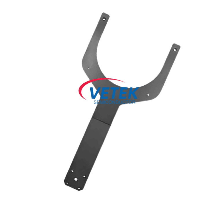
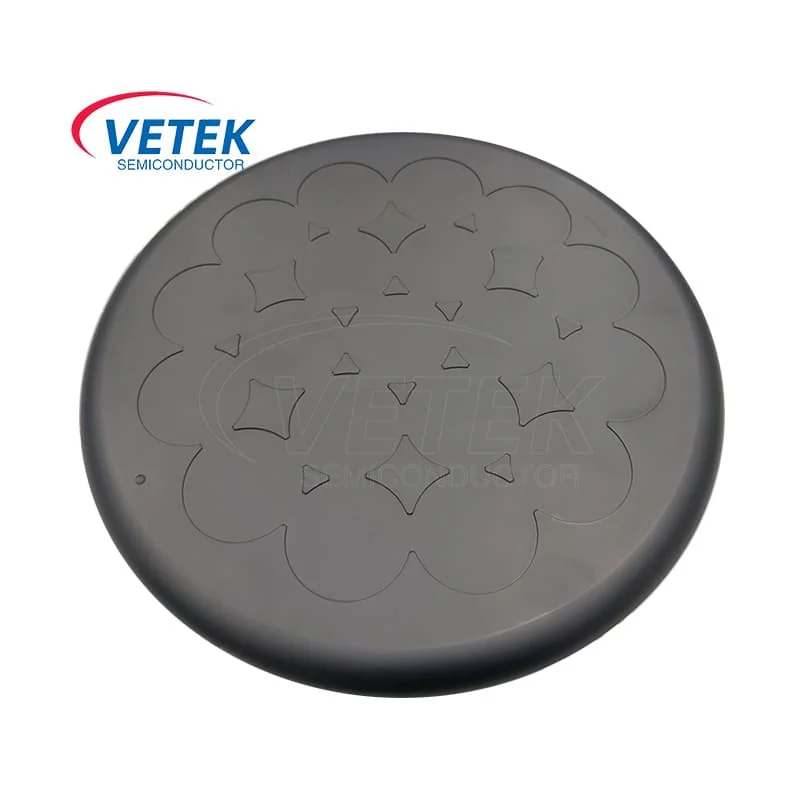
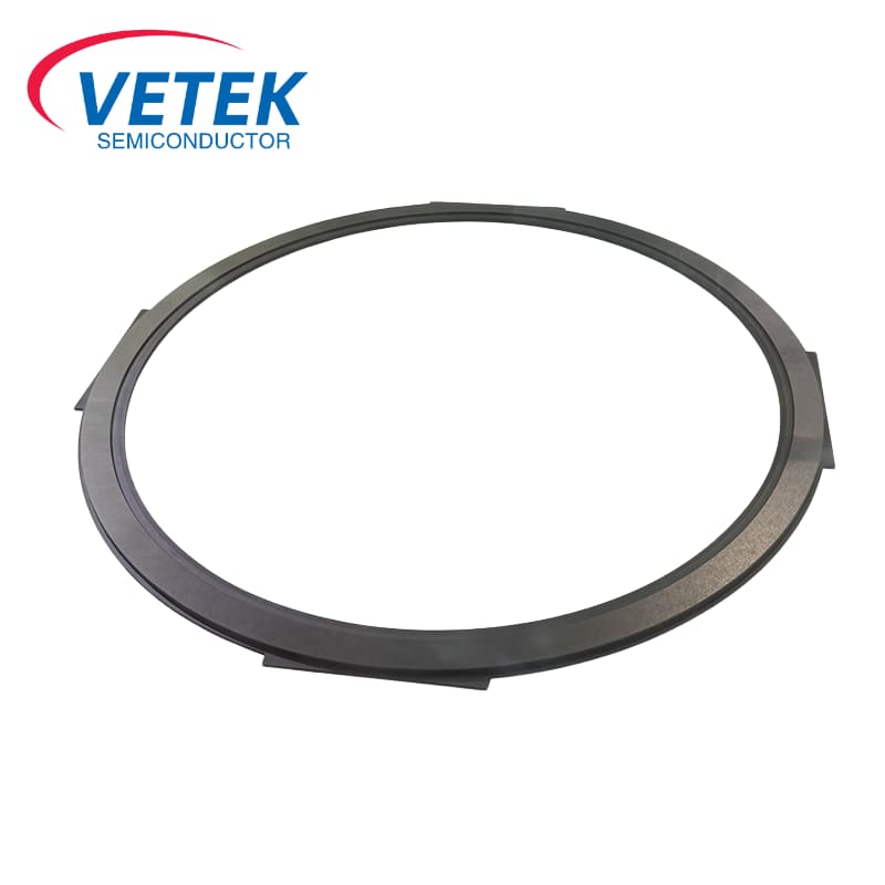
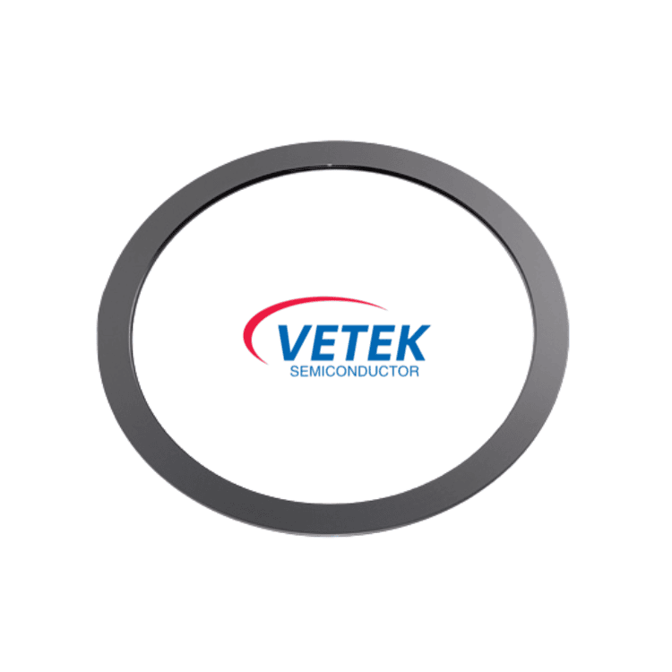
With this motto in mind, we've turn into one of quite possibly the most technologically innovative, cost-efficient, and price-competitive manufacturers for Pressureless Sintering Ceramic, SiC Ceramic Seal Ring, Pressureless Sintering SiC, Pressureless-Sintering-Silicon-Carbide-SSIC-Ceramic-Seal-Ring, Pressureless Sintering Silicon Carbide(SSIC), We have been sincerely wanting forward to cooperate with consumers all over the earth. We feel we can easily satisfy with you. We also warmly welcome buyers to visit our manufacturing unit and purchase our products and solutions.
Pressureless Sintering Ceramic, So that you can utilize the resource from the expanding info in international trade, we welcome shoppers from everywhere on-line and offline. In spite of the good quality solutions we present, effective and satisfying consultation service is supplied by our specialist after-sale service team. Product lists and comprehensive parameters and any other info weil be sent for you timely for your inquiries. So make sure you make contact with us by sending us emails or call us if you have any questions about our corporation. ou may also get our address info from our web page and come to our company to get a field survey of our merchandise. We have been confident that we are intending to share mutual achievement and create strong co-operation relations with our companions in this marketplace. We're searching forward for your inquiries.

Hot Products

  • Silicon Carbide Wafer Boat

    Silicon Carbide Wafer Boat

    VeTek Semiconductor's high-purity Silicon Carbide Wafer Boat is made of extremely pure silicon carbide material with excellent thermal stability, mechanical strength and chemical resistance. High-purity Silicon Carbide Wafer Boat is used in hot zone applications in semiconductor manufacturing, especially in high-temperature environments, and plays an important role in protecting wafers, transporting materials and maintaining stable processes. VeTek Semiconductor will continue to work hard to innovate and improve the performance of high-purity Silicon Carbide Wafer Boat to meet the evolving needs of semiconductor manufacturing. We look forward to becoming your long-term partner in China.Feel free to inquire us.
  • PSS Etching Carrier Plate for Semiconductor

    PSS Etching Carrier Plate for Semiconductor

    VeTek Semiconductor's PSS Etching Carrier Plate for Semiconductor is a high-quality, ultra-pure graphite carrier designed for wafer handling processes. Our carriers have excellent performance and can perform well in harsh environments, high temperatures and harsh chemical cleaning conditions. Our products are widely used in many European and American markets, and we look forward to becoming your long-term partner in China.You are welcome to come to China to visit our factory and learn more about our technology and products.
  • MOCVD epitaxial wafer susceptor

    MOCVD epitaxial wafer susceptor

    VeTek Semiconductor has been engaged in the semiconductor epitaxial growth industry for a long time and has rich experience and process skills in MOCVD epitaxial wafer susceptor products. Today, VeTek Semiconductor has become China's leading MOCVD epitaxial wafer susceptor manufacturer and supplier, and the wafer susceptors it provides have played an important role in the manufacturing of GaN epitaxial wafers and other products.
  • CVD SiC coating graphite susceptor

    CVD SiC coating graphite susceptor

    VeTek Semiconductor CVD SiC coating graphite susceptor is one of the important components in the semiconductor industry such as epitaxial growth and wafer processing. It is used in MOCVD and other equipment to support the processing and handling of wafers and other high-precision materials. VeTek Semiconductor has China's leading SiC coated graphite susceptor and TaC Coated Graphite Susceptor production and manufacturing capabilities, and looks forward to your consultation.
  • Ion Beam Sputter sources grid

    Ion Beam Sputter sources grid

    Ion beam is mainly used for ion etching, ion coating and plasma injection. The role of the Ion Beam Sputter sources grid is to dissect the ions and accelerate them to the required energy. Vetek Semiconductor provides high purity graphite ion beam Ion Beam Sputter sources grid for optical lens ion beam polishing, semiconductor wafer modification, etc. Welcome to inquire about customized products.
  • Porous SiC Ceramic Chuck

    Porous SiC Ceramic Chuck

    Vetek Semiconductor offers Porous SiC Ceramic Chuck widely used in wafer processing technology, transfer and other links, suitable for bonding, scribing, patch, polishing and other links, laser processing. Our Porous SiC Ceramic Chuck has Ultra-strong vacuum adsorption, high flatness and high purity meet the needs of most semiconductor industries.Welcome to inquiry us.

Send Inquiry

X
We use cookies to offer you a better browsing experience, analyze site traffic and personalize content. By using this site, you agree to our use of cookies. Privacy Policy
Reject Accept