


?")


QR Code

About Us
Products
Contact Us

Phone

Fax
+86-579-87223657

E-mail

Address
Wangda Road, Ziyang Street, Wuyi County, Jinhua City, Zhejiang Province, China


SiC is a wide bandgap semiconductor with excellent properties, in high demand for high-voltage, high-power, and high-frequency applications, especially in power semiconductors. SiC crystals are grown using the PVT method at a growth rate of 0.3 to 0.8 mm/h to control crystallinity. Rapid growth of SiC has been challenging due to quality issues such as carbon inclusions, purity degradation, polycrystalline growth, grain boundary formation, and defects like dislocations and porosity, limiting the productivity of SiC substrates.
Traditional silicon carbide raw materials are obtained by reacting high-purity silicon and graphite, which are high in cost, low in purity and small in size. VeTek Semiconductor uses fluidized bed technology and chemical vapor deposition to generate CVD SiC Block using methyltrichlorosilane. The main byproduct is only hydrochloric acid, which has low environmental pollution.
VeTek Semiconductor uses CVD SiC Block for SiC Crystal Growth. Ultra-high purity silicon carbide (SiC) produced through chemical vapor deposition (CVD) can be used as a source material for growing SiC crystals via physical vapor transport (PVT).
VeTek Semiconductor specializes in large-particle SiC for PVT, which has higher density compared to small-particle material formed by spontaneous combustion of Si and C-containing gases. Unlike solid-phase sintering or the reaction of Si and C, PVT does not require a dedicated sintering furnace or time-consuming sintering step in the growth furnace.
VeTek Semiconductor successfully demonstrated the PVT method for rapid SiC crystal growth under high-temperature gradient conditions using crushed CVD-SiC Blocks for SiC Crystal Growth. The grown raw material still maintains its prototype, reducing recrystallization, reducing raw material graphitization, reducing carbon wrapping defects, and improving crystal quality.
Raw materials and reaction mechanisms
Traditional toner/silica powder method: using high purity silica powder + toner as raw material, SiC crystal is synthesized at high temperature above 2000℃ by physical vapor transfer (PVT) method, which has high energy consumption and easy to introduce impurities.
CVD SiC particles: The vapor phase precursor (such as silane, methylsilane, etc.) is used to generate high-purity SiC particles by chemical vapor deposition (CVD) at a relatively low temperature (800-1100℃), and the reaction is more controllable and less impurities.
The CVD method can precisely regulate the SiC grain size (as low as 2 nm) to form an intercalated nanowire/tube structure, which significantly improves the density and mechanical properties of the material.
Anti-expansion performance optimization: Through the porous carbon skeleton silicon storage design, silicon particle expansion is limited to micropores, and the cycle life is more than 10 times higher than that of traditional silicon-based materials.
New energy field: Replace the traditional silicon carbon negative electrode, the first efficiency is increased to 90% (the traditional silicon oxygen negative electrode is only 75%), support 4C fast charge, to meet the needs of power batteries.
Semiconductor field: Grow 8 inches and above large size SiC wafer, crystal thickness up to 100mm (traditional PVT method only 30mm), yield increased by 40%.
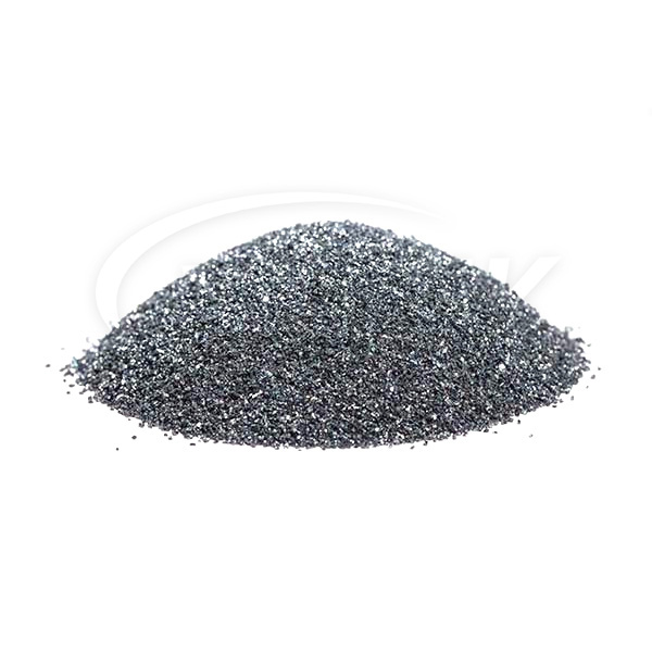
| Size | Part Number | Details |
| Standard | SC-9 | Particle Size(0.5-12mm) |
| Small | SC-1 | Particle Size(0.2-1.2mm) |
| Medium | SC-5 | Particle Size(1 -5mm) |
Purity excluding nitrogen: better than 99.9999%(6N)
| Element | Purity |
| B, AI, P | <1 ppm |
| Total metals | <1 ppm |


| Basic physical properties of CVD SiC coating | |
| Property | Typical Value |
| Crystal Structure | FCC β phase polycrystalline, mainly (111) oriented |
| SiC coating Density | 3.21 g/cm³ |
| CVD SiC coating Hardness | 2500 Vickers hardness(500g load) |
| Grain SiZe | 2~10μm |
| Chemical Purity | 99.99995% |
| Heat Capacity | 640 J·kg-1·K-1 |
| Sublimation Temperature | 2700℃ |
| Flexural Strength | 415 MPa RT 4-point |
| Young' s Modulus | 430 Gpa 4pt bend, 1300℃ |
| Thermal Conductivity | 300W·m-1·K-1 |
| Thermal Expansion(CTE) | 4.5×10⁻⁶K-1 |


Address
Wangda Road, Ziyang Street, Wuyi County, Jinhua City, Zhejiang Province, China
Tel
+86-579-87223657
Wangda Road, Ziyang Street, Wuyi County, Jinhua City, Zhejiang Province, China