Products

China LED Application Manufacturer, Supplier, Factory

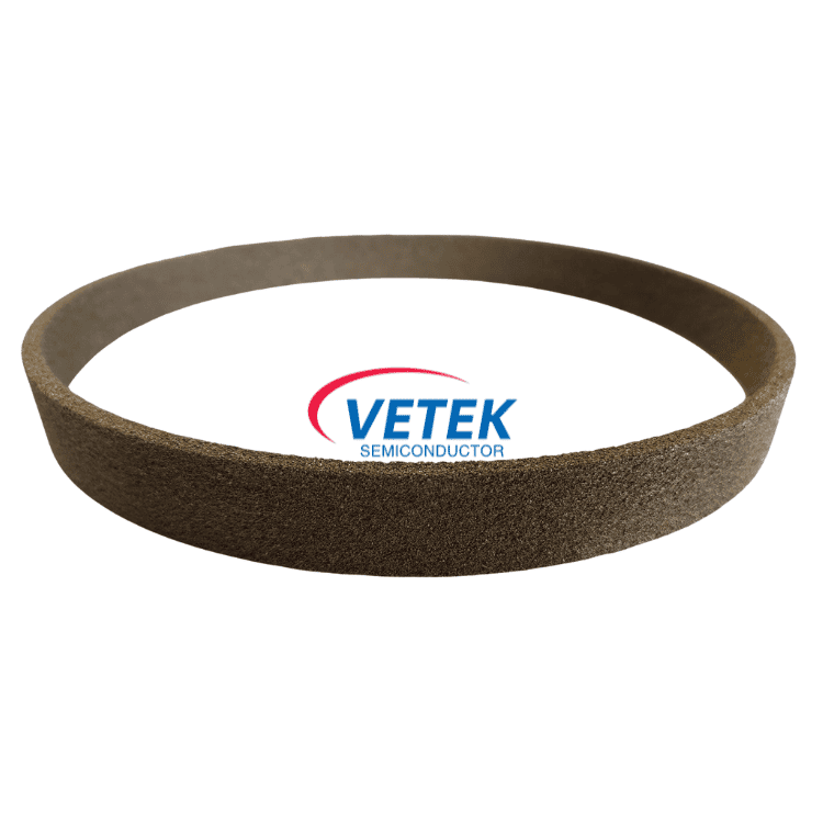
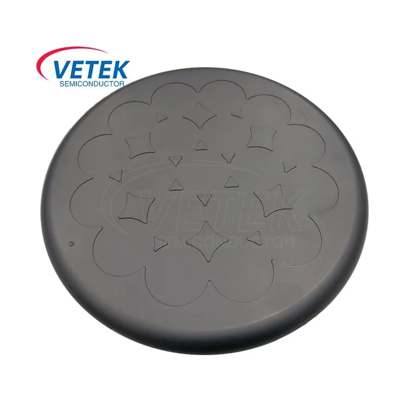
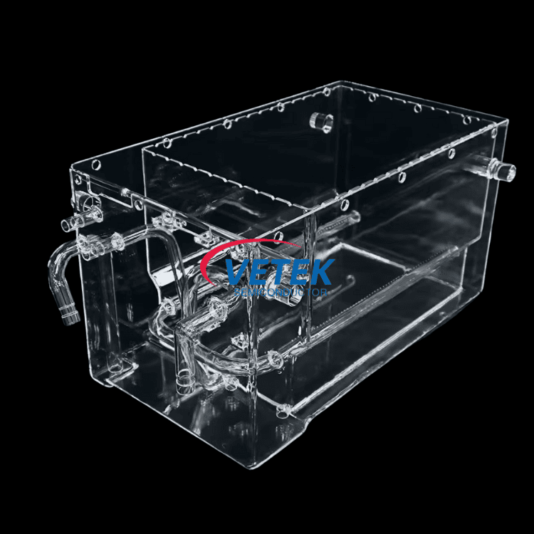
Dependable high-quality and fantastic credit standing are our principles, which will help us at a top-ranking position. Adhering to your tenet of "quality very first, client supreme" for LED Application, RTP Carrier Plate, RTP with a Carrier Plate, PSS Etching Process, Silicon Carbide, We welcome new and previous consumers from all walks of lifestyle to speak to us for upcoming business enterprise associations and mutual results!
LED Application, We pursue the management tenet of "Quality is superior, Service is supreme, Reputation is first", and will sincerely create and share success with all clients. We welcome you to contact us for more information and look forward to working with you.

Hot Products

  • TaC Coated Deflector Ring

    TaC Coated Deflector Ring

    VeTek Semiconductor's TaC Coated Deflector Ring is a highly specialized component designed for SiC crystal growth processes. The TaC coating provides excellent high temperature resistance and chemical inertness to cope with the high temperatures and corrosive environments during crystal growth process. This ensures stable performance and long life of the component, reducing the frequency of replacement and downtime. We are committed to providing quality products at competitive prices and look forward to being your long-term partner in China.Welcome to consult at any time.
  • SiC coating Monocrystalline silicon epitaxial tray

    SiC coating Monocrystalline silicon epitaxial tray

    SiC coating Monocrystalline silicon epitaxial tray is an important accessory for monocrystalline silicon epitaxial growth furnace, ensuring minimal pollution and stable epitaxial growth environment. VeTek Semiconductor's SiC coating Monocrystalline silicon epitaxial tray has an ultra-long service life and provides a variety of customization options. VeTek Semiconductor looks forward to becoming your long-term partner in China.
  • Chemical Vapor Deposition Process Solid SiC Edge Ring

    Chemical Vapor Deposition Process Solid SiC Edge Ring

    VeTek Semiconductor has always been committed to the research and development and manufacturing of advanced semiconductor materials. Today, VeTek Semiconductor has made great progress in Chemical Vapor Deposition Process Solid SiC Edge Ring products and is able to provide customers with highly customized solid SiC edge rings. Solid SiC edge rings provide better etching uniformity and precise wafer positioning when used with an electrostatic chuck, ensuring consistent and reliable etching results. Looking forward to your inquiry and becoming each other's long-term partners.
  • SiC Coating Collector Bottom

    SiC Coating Collector Bottom

    With our expertise in CVD SiC coating manufacturing, VeTek Semiconductor proudly presents Aixtron SiC Coating Collector Bottom,center and top. These SiC Coating Collector Bottom is constructed using high purity graphite and are coated with CVD SiC, ensuring impurity below 5ppm. Feel free to reach out to us for further information and inquiries.
  • Silicon Carbide Focus ring

    Silicon Carbide Focus ring

    Veteksemicon focus ring is designed specifically for demanding semiconductor etching equipment, particularly SiC etching applications. Mounted around the electrostatic chuck (ESC), in close proximity to the wafer, its primary function is to optimize the electromagnetic field distribution within the reaction chamber, ensuring uniform and focused plasma action across the entire wafer surface. A high-performance focus ring significantly improves etch rate uniformity and reduces edge effects, directly boosting product yield and production efficiency.
  • TaC Coating Rotation Susceptor

    TaC Coating Rotation Susceptor

    As a professional manufacturer, innovator and leader of TaC Coating Rotation Susceptor products in China. VeTek Semiconductor TaC Coating Rotation Susceptor is usually installed in chemical vapor deposition (CVD) and molecular beam epitaxy (MBE) equipment to support and rotate wafers to ensure uniform material deposition and efficient reaction. It is a key component in semiconductor processing. Welcome your further consultation.

Send Inquiry

X
We use cookies to offer you a better browsing experience, analyze site traffic and personalize content. By using this site, you agree to our use of cookies. Privacy Policy
Reject Accept