Products

China wafer handling Manufacturer, Supplier, Factory

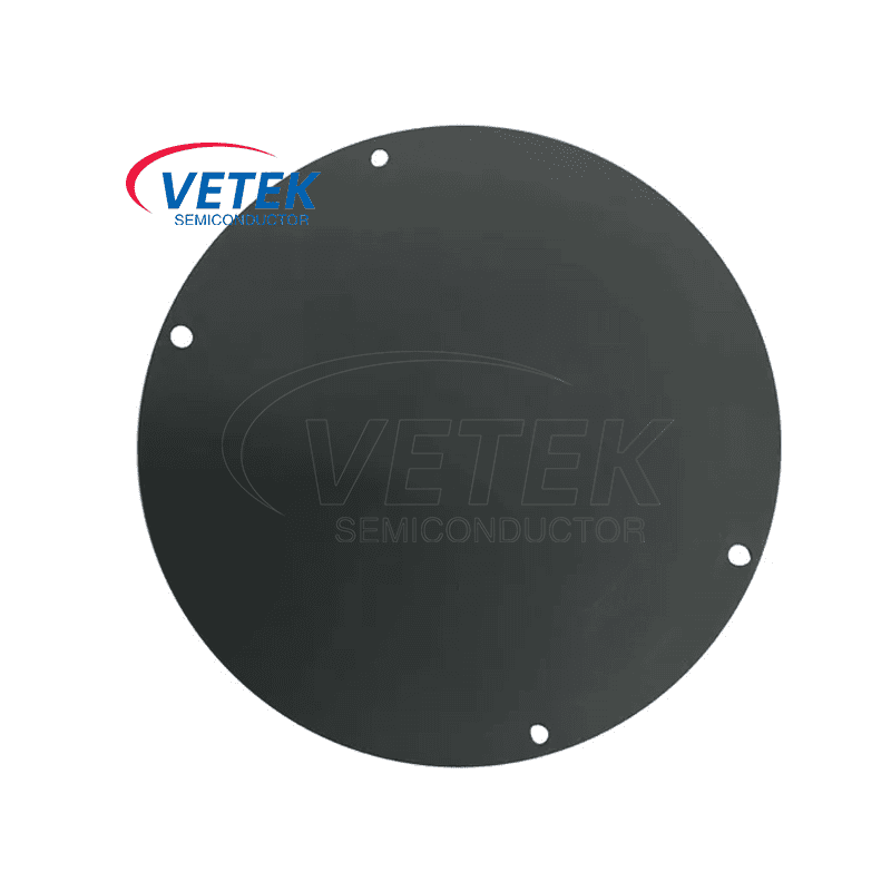
All we do is usually connected with our tenet " Client very first, Belief first, devoting about the food stuff packaging and environmental security for wafer handling, Wafer Handling End Effector, wafer handling equipment, wafer handling tools, wafer handling robot, As we're moving forward, we maintain an eye on our ever-expanding item range and make improvement to our expert services.
wafer handling, Our company mission is that providing high quality and beautiful products with reasonable price and strive to gain 100% good reputation from our clients. We believe Profession achieves excellence! We welcome you to cooperate with us and grow up together.

Hot Products

  • Alumina Ceramic Vacuum Chuck

    Alumina Ceramic Vacuum Chuck

    VeTek Semiconductor is a professional Alumina Ceramic Vacuum Chuck manufacturer and factory in China. Alumina Ceramic Vacuum Chuck uses high-purity aluminum oxide ceramics with excellent heat resistance, chemical resistance and mechanical strength. It is mainly used to fix and support wafers and substrates. It is a high-performance equipment for semiconductor processing. Welcome your further inquiries.
  • Fused Opaque Quartz

    Fused Opaque Quartz

    As a VeTek Semiconductor's fused opaque quartz features low transmittance and high thermal reflectivity, which can significantly reduce heat loss and thereby extend the life of heating components. Ultra-long service life, suitable for semiconductor heat treatment processes. VeTek Semiconductor is a professional supplier and manufacturer of fused opaque quartz and looks forward to becoming your long-term partner.
  • Three-petal Graphite Crucible

    Three-petal Graphite Crucible

    VeTek Semiconductor's Three-petal Graphite Crucible is made of high purity graphite material processed by surface pyrolytic carbon coating, which is used to pull single crystal thermal field. Compared with traditional crucible, the structure of three-lobe design is more convenient to install and disassemble, improve work efficiency, and the impurities below 5ppm can meet the application of semiconductor and photovoltaic industry.
  • Plasma Etching Focus Ring

    Plasma Etching Focus Ring

    An important component used in the wafer fabrication etching process is the plasma etching focus ring, whose function is to hold the wafer in place to maintain plasma density and prevent contamination of the wafer sides.Vetek semiconductor provide plasma etching focus ring with different material like monocrystalline silicon, silicon carbide, boron carbide and other ceramic materials.
  • Silicon Carbide (SiC) Cantilever Paddle

    Silicon Carbide (SiC) Cantilever Paddle

    The role of Silicon Carbide (SiC) Cantilever Paddle in the semiconductor industry is to support and transport wafers. In high-temperature processes such as diffusion and oxidation, SiC cantilever paddle can stably carry wafer boats and wafers without deformation or damage due to high temperature, ensuring the smooth progress of the process. Making diffusion, oxidation and other processes more uniform is crucial to improving the consistency and yield of wafer processing. VeTek Semiconductor uses advanced technology to build SiC cantilever paddle with high-purity silicon carbide to ensure that wafers will not be contaminated. VeTek Semiconductor looks forward to long-term cooperation with you on Silicon Carbide (SiC) Cantilever Paddle products.
  • C/C Composite Crucible

    C/C Composite Crucible

    Designed for the harsh environment of silicon single crystal production, the C/C Composite Crucible is an indispensable component of the semiconductor silicon single crystal production process.

Send Inquiry

X
We use cookies to offer you a better browsing experience, analyze site traffic and personalize content. By using this site, you agree to our use of cookies. Privacy Policy
Reject Accept