
Products

China LED Wafer Handling Manufacturer, Supplier, Factory

We have now our possess revenue group, design staff, technical crew, QC team and package group. We now have strict excellent regulate procedures for each process. Also, all of our workers are experienced in printing subject for LED Wafer Handling, Quartz Wafer Boat, Semiconductor Diffusion, Solar Cell Quartz Boat, High Purity Quartz, we could solve our customer problems asap and do the profit for our customer. For those who need superior provider and excellent , pls choose us , thanks !
LED Wafer Handling, All styles appear on our website are for customizing. We meet up to individual requirements with all solutions of your very own styles. Our concept is to help presenting the confidence of each buyers with the offering of our most sincere service, and the right product.
Hot Products

  • CVD SiC Coating Protector

    CVD SiC Coating Protector

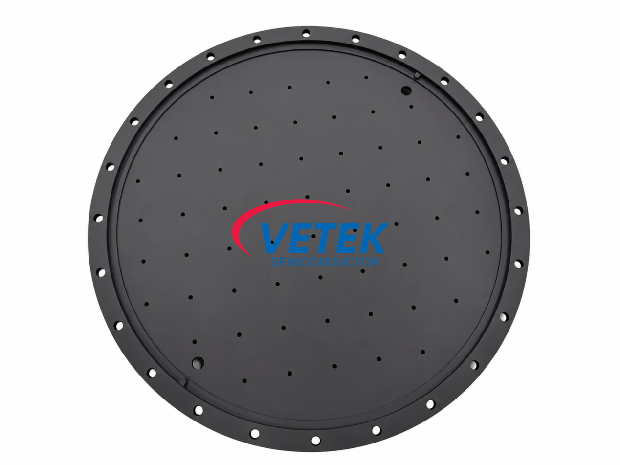
    Vetek Semiconductor's CVD SiC Coating Protector used is LPE SiC epitaxy, The term "LPE" usually refers to Low Pressure Epitaxy (LPE) in Low Pressure Chemical Vapor Deposition (LPCVD). In semiconductor manufacturing, LPE is an important process technology for growing single crystal thin films, often used to grow silicon epitaxial layers or other semiconductor epitaxial layers.Pls no hesitate to contact us for more questions.
  • Large sized resistance heating SiC crystal growth furnace

    Large sized resistance heating SiC crystal growth furnace

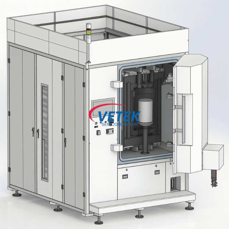
    Silicon carbide crystal growth is a core process in the manufacturing of high-performance semiconductor devices. The stability, precision, and compatibility of crystal growth equipment directly determine the quality and yield of silicon carbide ingots. Based on the characteristics of Physical Vapor Transport (PVT) technology, Veteksemi has developed a resistance heating furnace for silicon carbide crystal growth, enabling stable growth of 6-inch, 8-inch, and 12-inch silicon carbide crystals with full compatibility with conductive, semi-insulating, and N-type material systems. Through precise control of temperature, pressure, and power, it effectively reduces crystal defects such as EPD (Etch Pit Density) and BPD (Basal Plane Dislocation), while featuring low energy consumption and a compact design to meet the high standards of industrial large-scale production.
  • Aluminum Nitride ceramic Disc

    Aluminum Nitride ceramic Disc

    Vetek Semiconductor aluminum nitride ceramics disc is a high-performance material known for its excellent properties of high thermal conductivity & electrical insulation, especially suitable for demanding electrical applications. Aluminum nitride ceramic discs are stable at high temperatures in a variety of inert environments. Welcome to communicate with us.
  • CVD SiC coated wafer susceptor

    CVD SiC coated wafer susceptor

    Veteksemicon’s CVD SiC coated wafer susceptor is a cutting-edge solution for semiconductor epitaxial processes, offering ultra-high purity (≤100ppb, ICP-E10 certified) and exceptional thermal/chemical stability for contamination-resistant growth of GaN, SiC, and silicon-based epi-layers. Engineered with precision CVD technology, it supports 6”/8”/12” wafers, ensures minimal thermal stress, and withstands extreme temperatures up to 1600°C.
  • Wafer Handling Robotic Arm

    Wafer Handling Robotic Arm

    Vetek Semiconductor thermal spraying technology plays a vital role in the application of wafer handling robotic arms, especially in semiconductor manufacturing environments that require high precision and high cleanliness. This technology significantly improves the durability, reliability and work efficiency of the equipment by coating special materials on the surface of the wafer handling robotic arm. Welcome to inquiry us.
  • Tantalum Carbide Coated Guide Ring

    Tantalum Carbide Coated Guide Ring

    As a China leading TaC coating guide ring supplier and manufacturer, VeTek Semiconductor tantalum carbide coated guide ring is an important component used to guide and optimize the flow of reactive gases in the PVT (Physical Vapor Transport) method. It promotes the uniform deposition of SiC single crystals in the growth zone by adjusting the distribution and speed of the gas flow. VeTek Semiconductor is a leading manufacturer and supplier of TaC coating guide rings in China and even in the world, and we look forward to your consultation.

Send Inquiry

X
We use cookies to offer you a better browsing experience, analyze site traffic and personalize content. By using this site, you agree to our use of cookies.Privacy Policy
RejectAccept