
Products

China SiC Wafer Handling Manufacturer, Supplier, Factory

We have been ready to share our knowledge of internet marketing worldwide and recommend you suitable merchandise at most aggressive rates. So Profi Tools present you very best price of money and we are ready to develop alongside one another with SiC Wafer Handling, Ceramic Vacuum Chuck for wafer, Ceramic Vacuum Chuck, Semiconductor Wafer Chuck, Vacuum Chuck for Wafer Processing, For additional information and facts, please speak to us as quickly as possible!
SiC Wafer Handling, Hard work to keep making progress, innovation in the industry, make every effort to first-class enterprise. We try our best to build the scientific management model, to learn abundant expert knowledge, to develop advanced production equipment and production process , to create the first-call quality merchandise, reasonable price , high quality of service , quick delivery , to present you create new value .

Hot Products

  • SiC Coated Graphite Crucible Deflector

    SiC Coated Graphite Crucible Deflector

    The SiC coated graphite crucible deflector is a key component in the single crystal furnace equipment, its task is to guide the molten material from the crucible to the crystal growth zone smoothly, and ensure the quality and shape of the single crystal growth.Vetek semiconductor can provide both graphite and SiC coating material.Welcome to contact us for more details.
  • Monocrystalline pulling Crucible

    Monocrystalline pulling Crucible

    Graphite crucible is an important part of Monocrystalline Pulling Crucibles in the process of achieving monocrystalline silicon ingot growth.Vetek semiconductor's crucibles are intricately engineered to meet the rigorous requirements set by the semiconductor industry.We are committed to producing and supplying crystal growth graphite crucibles that excel in performance, quality, and cost-effectiveness to meet the evolving needs of the industry.Welcome to inquiry us.
  • Semiconductor thermal spraying technology

    Semiconductor thermal spraying technology

    Vetek Semiconductor Semiconductor thermal spraying technology is an advanced process that sprays materials in a molten or semi-molten state onto the surface of a substrate to form a coating. This technology is widely used in the field of semiconductor manufacturing, mainly used to create coatings with specific functions on the surface of the substrate, such as conductivity, insulation, corrosion resistance, and oxidation resistance. The main advantages of thermal spraying technology include high efficiency, controllable coating thickness, and good coating adhesion, making it particularly important in the semiconductor manufacturing process that requires high precision and reliability. Looking forward to your inquiry.
  • SiC Ceramics Membrane

    SiC Ceramics Membrane

    Veteksemicon SiC ceramics membranes are a type of inorganic membrane and belong to solid membrane materials in membrane separation technology. SiC membranes are fired at a temperature above 2000℃. The surface of the particles is smooth and round. There are no closed pores or channels in the support layer and each layer. They are usually composed of three layers with different pore sizes.
  • CVD SiC Pancake Susceptor

    CVD SiC Pancake Susceptor

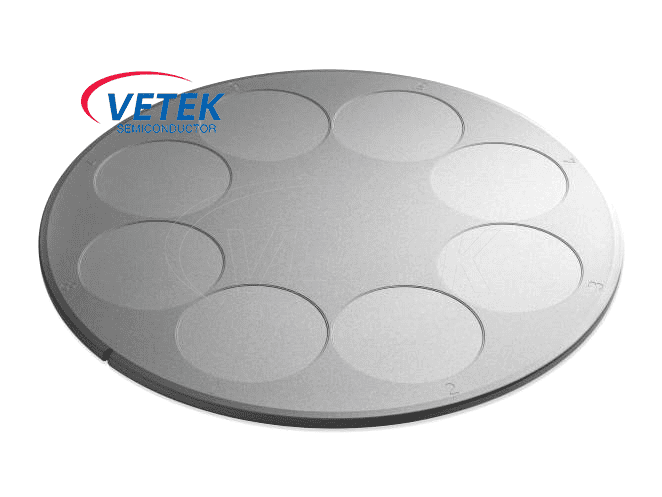
    As a leading manufacturer and innovator of CVD SiC Pancake Susceptor products in China. VeTek Semiconductor CVD SiC Pancake Susceptor, as a disc-shaped component designed for semiconductor equipment, is a key element to support thin semiconductor wafers during high-temperature epitaxial deposition. VeTek Semiconductor is committed to providing high-quality SiC Pancake Susceptor products and becoming your long-term partner in China at competitive prices.
  • Aixtron Satellite wafer carrier

    Aixtron Satellite wafer carrier

    VeTek Semiconductor’s Aixtron Satellite Wafer Carrier is a wafer carrier used in AIXTRON equipment, mainly used in MOCVD processes, and is particularly suitable for high-temperature and high-precision semiconductor processing processes. The carrier can provide stable wafer support and uniform film deposition during MOCVD epitaxial growth, which is essential for the layer deposition process. Welcome your further consultation.

Send Inquiry

X
We use cookies to offer you a better browsing experience, analyze site traffic and personalize content. By using this site, you agree to our use of cookies. Privacy Policy
Reject Accept