Products

China Quartz Crucible for Monocrystalline Silicon Manufacturer, Supplier, Factory

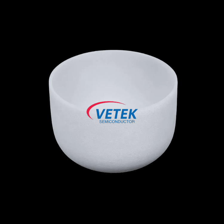
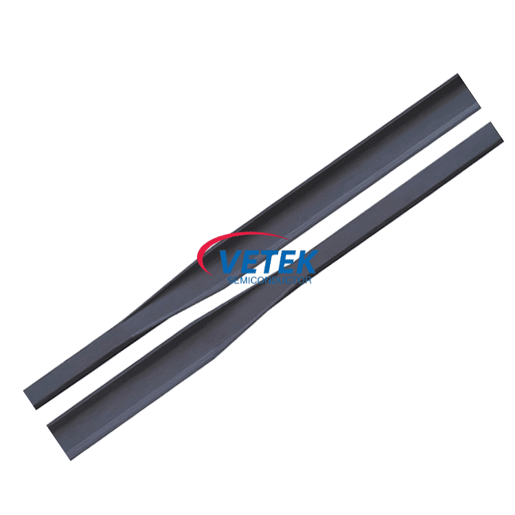
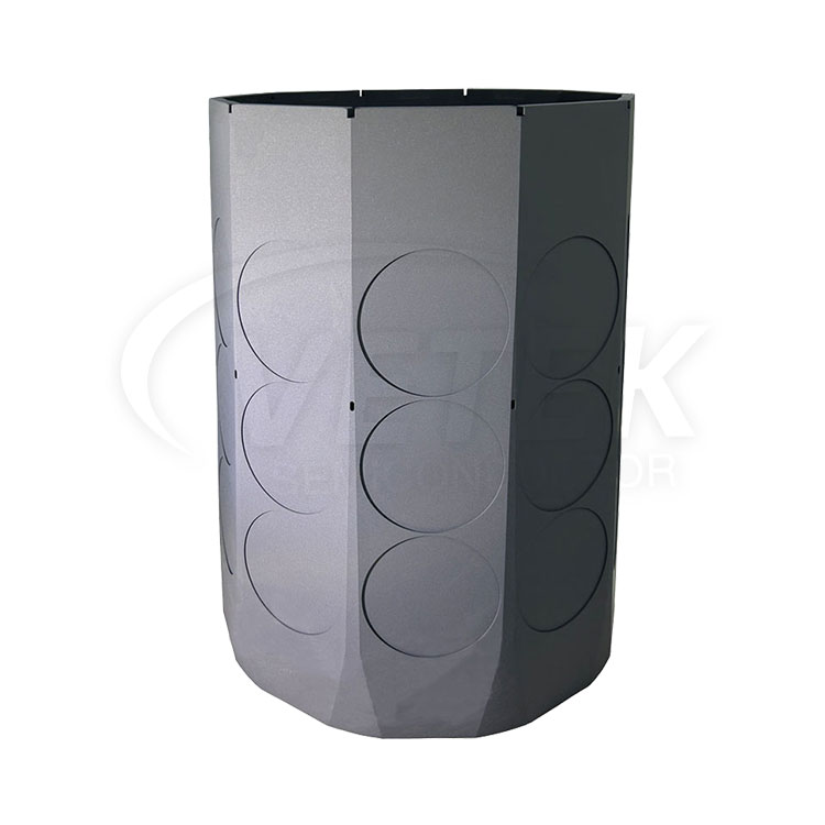
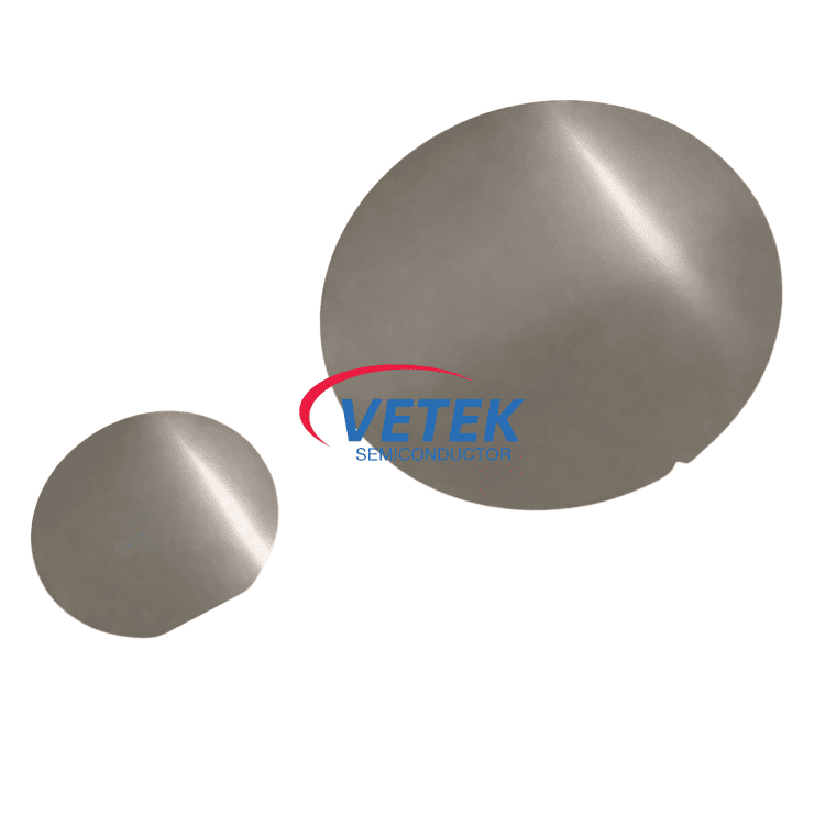
In the past few years, our company absorbed and digested advanced technologies both at home and abroad. Meanwhile, our company staffs a team of experts devoted to the development of Quartz Crucible for Monocrystalline Silicon, Semiconductor Quartz Crucible, Quartz Crucible for Semiconductor, CZ Quartz Crucible, Silicon Pulling Quartz Crucible, Now we have a skilled team for international trade. We will solve the problem you meet. We can present the goods you want. Be sure to feel cost-free to contact us.
Quartz Crucible for Monocrystalline Silicon, We always stick to the tenet of "sincerity, high quality, high efficiency, innovation". With years of efforts, we've got established friendly and stable business relationships with worldwide customers. We welcome any of your inquiries and concerns for our solutions, and we're sure that we are going to offer just what you want, as we always believe that your satisfaction is our success.

Hot Products

  • TaC Coated Graphite Wafer Carrier

    TaC Coated Graphite Wafer Carrier

    VeTek Semiconductor has carefully designed TaC Coated Graphite Wafer Carrier for customers. It is composed of high-purity graphite and TaC coating, which is suitable for various wafer epitaxial wafer processing. We have been specialized in SiC and TaC coating for many years. Compared with SiC coating, Our TaC coated graphite wafer carrier has a higher temperature resistance and wear-resistant. We look forward to becoming your long-term partner in China.
  • Wafer Chuck

    Wafer Chuck

    Wafer chunk a wafer clamping tool in semiconductor process and is widely used in PVD, CVD, ETCH and other process.Vetek Semiconductor's wafer chuck play pivotal roles in semiconductor production, enabling fast, high-quality output. With in-house manufacturing, competitive pricing, and robust R&D support, Vetek Semiconductor excels in OEM/ODM services for precision components.Looking forward to your inquiry.
  • TaC Coated Chuck

    TaC Coated Chuck

    With its high temperature resistance, chemical inertness and excellent performance, VeTek Semiconductor's TaC coated chucks are designed for semiconductor furnaces. We believe that our products can bring you advanced technology and quality product solutions.
  • High purity Rigid felt tube

    High purity Rigid felt tube

    VeTek Semiconductor high purity rigid felt tubes are the first choice for high-temperature applications in the semiconductor industry. Their high compressive strength and excellent thermal insulation properties make them reliable and efficient components in the crystal growth process. VeTek Semiconductor has always been committed to providing advanced and reliable high-purity rigid felt tube technology and product solutions for the semiconductor industry. We welcome your further inquiries.
  • Silicon Carbide SiC wafer boat

    Silicon Carbide SiC wafer boat

    Veteksemicon SiC wafer boats are widely used in critical high-temperature processes in semiconductor manufacturing, serving as reliable carriers for oxidation, diffusion, and annealing processes for silicon-based integrated circuits. They also excel in the third-generation semiconductor sector, perfectly suited for demanding processes such as epitaxial growth (EPI) and metal-organic chemical vapor deposition (MOCVD) for SiC and GaN power devices. They also support the high-temperature fabrication of high-efficiency solar cells in the photovoltaic industry. Looking forward to your further consultation.
  • CVD TaC Coated Graphite Ring

    CVD TaC Coated Graphite Ring

    The CVD TaC Coated Graphite Ring by Veteksemicon is engineered to meet the extreme demands of semiconductor wafer processing. Utilizing Chemical Vapor Deposition (CVD) technology, a dense and uniform Tantalum Carbide (TaC) coating is applied to high-purity graphite substrates, achieving exceptional hardness, wear resistance, and chemical inertness. In semiconductor fabrication, the CVD TaC Coated Graphite Ring is widely used in MOCVD, etching, diffusion, and epitaxial growth chambers, serving as a key structural or sealing component for wafer carriers, susceptors, and shielding assemblies. Looking forward to your further consultation.

Send Inquiry

X
We use cookies to offer you a better browsing experience, analyze site traffic and personalize content. By using this site, you agree to our use of cookies. Privacy Policy
Reject Accept