Products

China High purity SiN susbstrate Manufacturer, Supplier, Factory

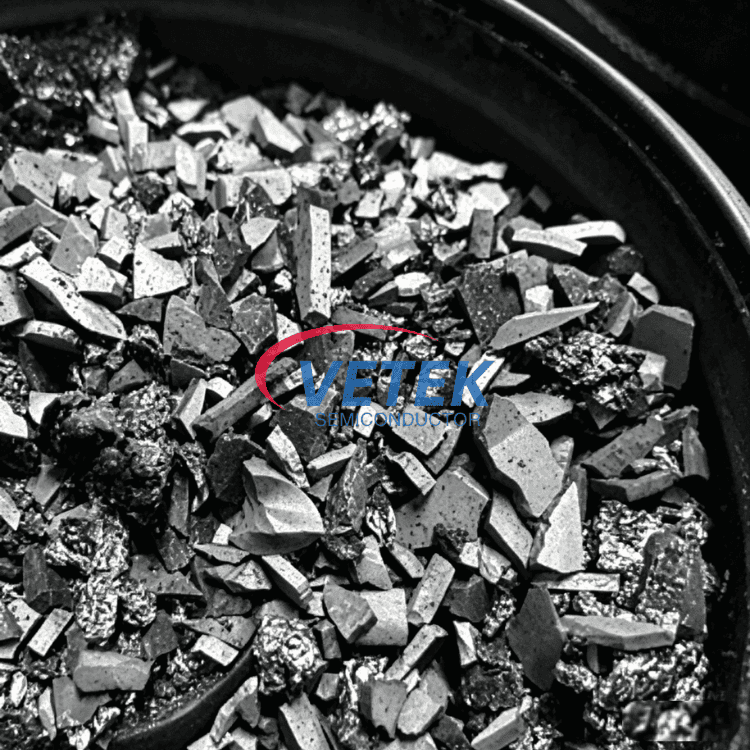
We support our consumers with ideal high-quality goods and substantial level support. Becoming the specialist manufacturer in this sector, we now have acquired abundant practical encounter in producing and managing for High purity SiN susbstrate, SiN susbstrate, Silicon Nitride, Silicon Nitride susbstrate, SiN Substrates, Please truly feel absolutely free to call us at any time. We will reply you when we receive your inquiries. Please note that samples are available before we start our company.
High purity SiN susbstrate, When It produced, it making use of the world's major method for reliable operation, a low failure price, it appropriate for Jeddah shoppers choice. Our enterprise. s situated inside the national civilized cities, the website traffic is very hassle-free, unique geographical and financial circumstances. We pursue a "people-oriented, meticulous manufacturing, brainstorm, make brilliant" company philosophy. Strict good quality management, fantastic service, affordable cost in Jeddah is our stand around the premise of competitors. If needed, welcome to make contact with us by our web page or phone consultation, we'll be delighted to serve you.

Hot Products

  • Wafer Handling End Effector

    Wafer Handling End Effector

    Wafer Handling End Effector is an important part in the semiconductor processing, transporting wafers and protecting their surfaces from damage. VeTek Semiconductor, as a leading manufacturer and supplier of Wafer Handling End Effector, is always committed to providing customers with excellent Wafer Handling Robotic Arm products and the best services. we look forward to becoming your long-term partner in wafer handling tools products.
  • TaC Coating Guide Ring

    TaC Coating Guide Ring

    VeTek Semiconductor's TaC Coating Guide Ring is created by applying tantalum carbide coating onto graphite parts using a highly advanced technique called chemical vapor deposition (CVD). This method is well-established and offers exceptional coating properties. By utilizing the TaC Coating Guide Ring, the lifespan of graphite components can be significantly extended, the movement of graphite impurities can be suppressed, and the SiC and AIN single crystal quality can be reliably maintained. Welcome to inquiry us.
  • CVD SiC Coating Nozzle

    CVD SiC Coating Nozzle

    CVD SiC Coating Nozzles are crucial components used in the LPE SiC epitaxy process for depositing silicon carbide materials during semiconductor manufacturing. These nozzles are typically made of high-temperature and chemically stable silicon carbide material to ensure stability in harsh processing environments. Designed for uniform deposition, they play a key role in controlling the quality and uniformity of epitaxial layers grown in semiconductor applications. Welcome your further inquiry.
  • Wafer Chuck

    Wafer Chuck

    Wafer chunk a wafer clamping tool in semiconductor process and is widely used in PVD, CVD, ETCH and other process.Vetek Semiconductor's wafer chuck play pivotal roles in semiconductor production, enabling fast, high-quality output. With in-house manufacturing, competitive pricing, and robust R&D support, Vetek Semiconductor excels in OEM/ODM services for precision components.Looking forward to your inquiry.
  • Si EPI Susceptor

    Si EPI Susceptor

    China top factory-Vetek Semiconductor combines precision machining and semiconductor SiC and TaC coating capabilities. The barrel type Si Epi Susceptor provides temperature and atmosphere control capabilities, enhancing production efficiency in semiconductor epitaxial growth processes.Looking forward to setting up cooperation relationship with you.
  • Tantalum Carbide Ring

    Tantalum Carbide Ring

    As an advanced manufacturer and producer of Tantalum Carbide Ring products in China, VeTek Semiconductor Tantalum Carbide Ring has extremely high hardness, wear resistance, high temperature resistance and chemical stability, and is widely used in the semiconductor manufacturing field. Especially in CVD, PVD, ion implantation process, etching process, and wafer processing and transportation, it is an indispensable product for semiconductor processing and manufacturing. Looking forward to your further consultation.

Send Inquiry

X
We use cookies to offer you a better browsing experience, analyze site traffic and personalize content. By using this site, you agree to our use of cookies. Privacy Policy
Reject Accept