




QR Code

Products
Contact Us


Fax
+86-579-87223657

E-mail

Address
Wangda Road, Ziyang Street, Wuyi County, Jinhua City, Zhejiang Province, China


• Semiconductor-grade dehydroxylated fused quartz with SiO₂ ≥ 99.999% and tightly controlled metallic impurities
• Stable continuous operation up to 1100 °C, with short-term capability near 1200 °C
• Strong resistance to fluorine- and chlorine-based etch chemistries and high-energy plasma exposure
• Low thermal expansion and good thermal-shock performance under repeated chamber temperature cycles
• Low vacuum outgassing to protect chamber base pressure and process gas composition
• Micron-level dimensional control with polished contact surfaces for consistent chamber fit and plasma boundary definition
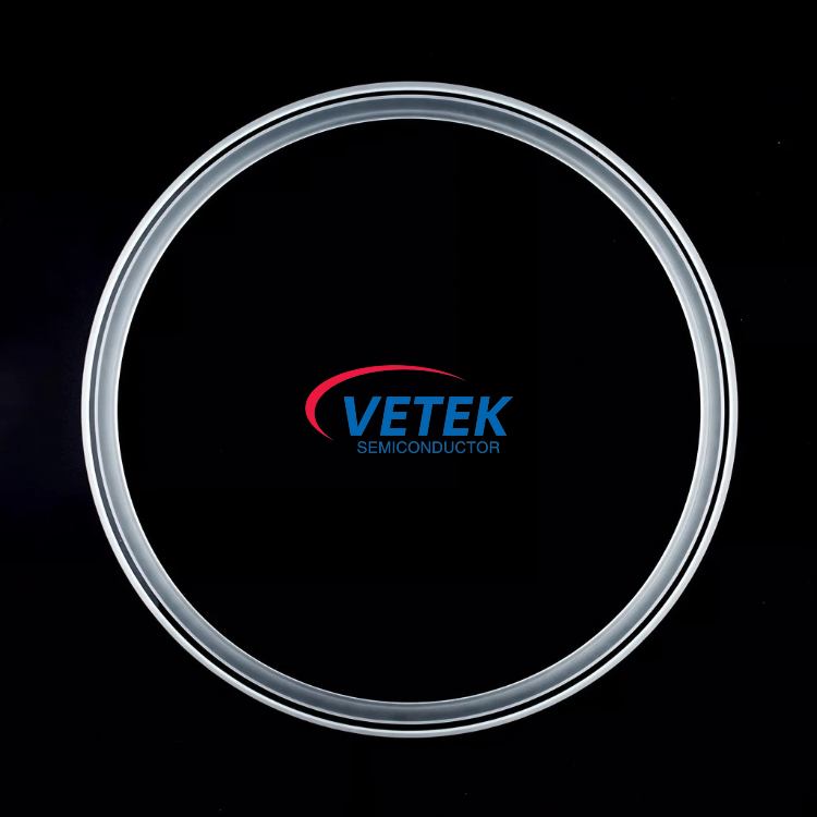
• Configurable designs: flat rings, stepped etch rings, locating/retaining rings, and fully custom profiles for major etch tool platforms
High Purity Quartz Etch Rings are used in dry plasma etch process chambers for:
• Logic and memory device plasma etch steps
• SiC and GaN power-device etch processes
• High-aspect-ratio structure etch
• Optical and compound-semiconductor substrate plasma processing
• Advanced packaging plasma etch and related cleaning steps
• RIE / ICP laboratory and production etch tools
• Material: semiconductor-grade dehydroxylated fused quartz, SiO₂ ≥ 99.999%
• Wafer compatibility: 2 / 4 / 6 / 8 / 12 inch silicon, SiC, GaN, and sapphire
• Operating temperature: −20 °C to 1100 °C continuous; short-term peak approximately 1200 °C
• Primary functions: plasma edge confinement, gas-flow guidance, edge protection, and chamber isolation
• Machining quality: micron-level tolerances, polished surfaces, controlled edges, and clean finish
• Structure options: flat ring, stepped etch ring, locating/retaining ring, and custom geometries
• Customization: outer/inner diameter, thickness, step height, locating features, chamfers, and interface details per drawing
VeTek Semiconductor supplies process-critical quartz hardware for etch and thermal tools. For etch rings, the focus is on:
• Material purity and surface cleanliness suited to advanced dry-etch environments
• Dimensional accuracy that supports stable plasma boundary control and repeatable chamber fit
• Design flexibility for OEM-style replacement and fully custom chamber interfaces
• A complete quartz component range that also includes wafer carriers, furnace tubes, boats, and related process parts
By combining high purity, plasma durability, and tight geometry control, VeTek High Purity Quartz Etch Rings help improve across-wafer etch uniformity, reduce edge-related defects, and support longer, more stable production cycles in dry plasma etch tools.
Address
Wangda Road, Ziyang Street, Wuyi County, Jinhua City, Zhejiang Province, China
Tel
+86-579-87223657
Wangda Road, Ziyang Street, Wuyi County, Jinhua City, Zhejiang Province, China