Products

China rigid felt for Crystal Growth Manufacturer, Supplier, Factory

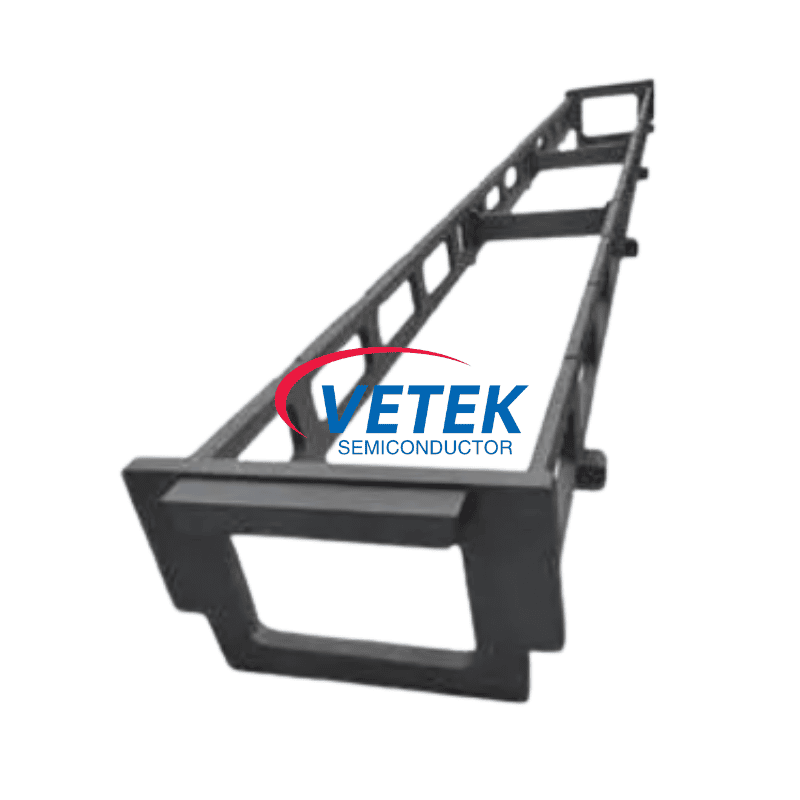
Our growth depends within the innovative equipment, fantastic talents and repeatedly strengthened technology forces for rigid felt for Crystal Growth, Sapphire Crystal Growth rigid felt, Sapphire Crystal Growth hard felt, Sapphire Crystal Growth Insulator, SiC Crystal Growth, Our experienced specialized workforce will probably be wholeheartedly at your provider. We sincerely welcome you to check out our web-site and organization and mail us your inquiry.
rigid felt for Crystal Growth, During the development, our company has built a well-known brand. It is well highly acclaimed by our customers. OEM and ODM are accepted. We are looking forward to customers from all over the world to join us to a wild cooperation.

Hot Products

  • Monocrystalline pulling Crucible

    Monocrystalline pulling Crucible

    Graphite crucible is an important part of Monocrystalline Pulling Crucibles in the process of achieving monocrystalline silicon ingot growth.Vetek semiconductor's crucibles are intricately engineered to meet the rigorous requirements set by the semiconductor industry.We are committed to producing and supplying crystal growth graphite crucibles that excel in performance, quality, and cost-effectiveness to meet the evolving needs of the industry.Welcome to inquiry us.
  • Semiconductor Ceramic Nozzle

    Semiconductor Ceramic Nozzle

    Semiconductor ceramic nozzle from VeTeK Semiconductor are carefully manufactured with excellent uniformity and precision. As a professional Semiconductor ceramic nozzle manufacturer and supplier, VeTeKSemi is always committed to providing the highest quality Ceramic Nozzle products at competitive prices. Welcome your further consultation.
  • Physical Vapor Deposition

    Physical Vapor Deposition

    Vetek semiconductor Physical Vapor Deposition (PVD) is an advanced process technology widely used in surface treatment and thin film preparation. PVD technology uses physical methods to directly transform materials from solid or liquid to gas and form a thin film on the surface of the target substrate. This technology has the advantages of high precision, high uniformity and strong adhesion, and is widely used in semiconductors, optical devices, tool coatings and decorative coatings. Welcome to discuss with us!
  • UV LED Epi Susceptor

    UV LED Epi Susceptor

    As a China leading semiconductor susceptor product manufacturer and leader, VeTek Semiconductor has been focusing on various types of suceptor products such as UV LED Epi Susceptor, SiC Coating Susceptor, MOCVD Susceptor. VeTekSemi supports customized product services and looks forward to your consultation.
  • Plasma Etching Focus Ring

    Plasma Etching Focus Ring

    An important component used in the wafer fabrication etching process is the plasma etching focus ring, whose function is to hold the wafer in place to maintain plasma density and prevent contamination of the wafer sides.Vetek semiconductor provide plasma etching focus ring with different material like monocrystalline silicon, silicon carbide, boron carbide and other ceramic materials.
  • 4°off axis p-type SiC Wafer

    4°off axis p-type SiC Wafer

    VeTek Semiconductor is a professional Chinese manufacturer of 4°off axis p-type SiC Wafer. 4°off axis p-type SiC Wafer is a special semiconductor material used in high-performance electronic devices. VeTek Semiconductor is committed to providing advanced solutions for various SiC Wafer products. We sincerely look forward to your further consultation.

Send Inquiry

X
We use cookies to offer you a better browsing experience, analyze site traffic and personalize content. By using this site, you agree to our use of cookies. Privacy Policy
Reject Accept