




QR Code

Products
Contact Us


Fax
+86-579-87223657

Email

Address
Wangda Road, Ziyang Street, Wuyi County, Jinhua City, Zhejiang Province, China


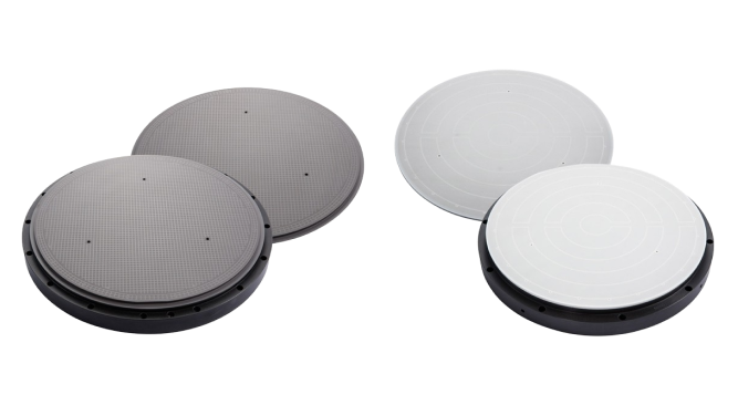
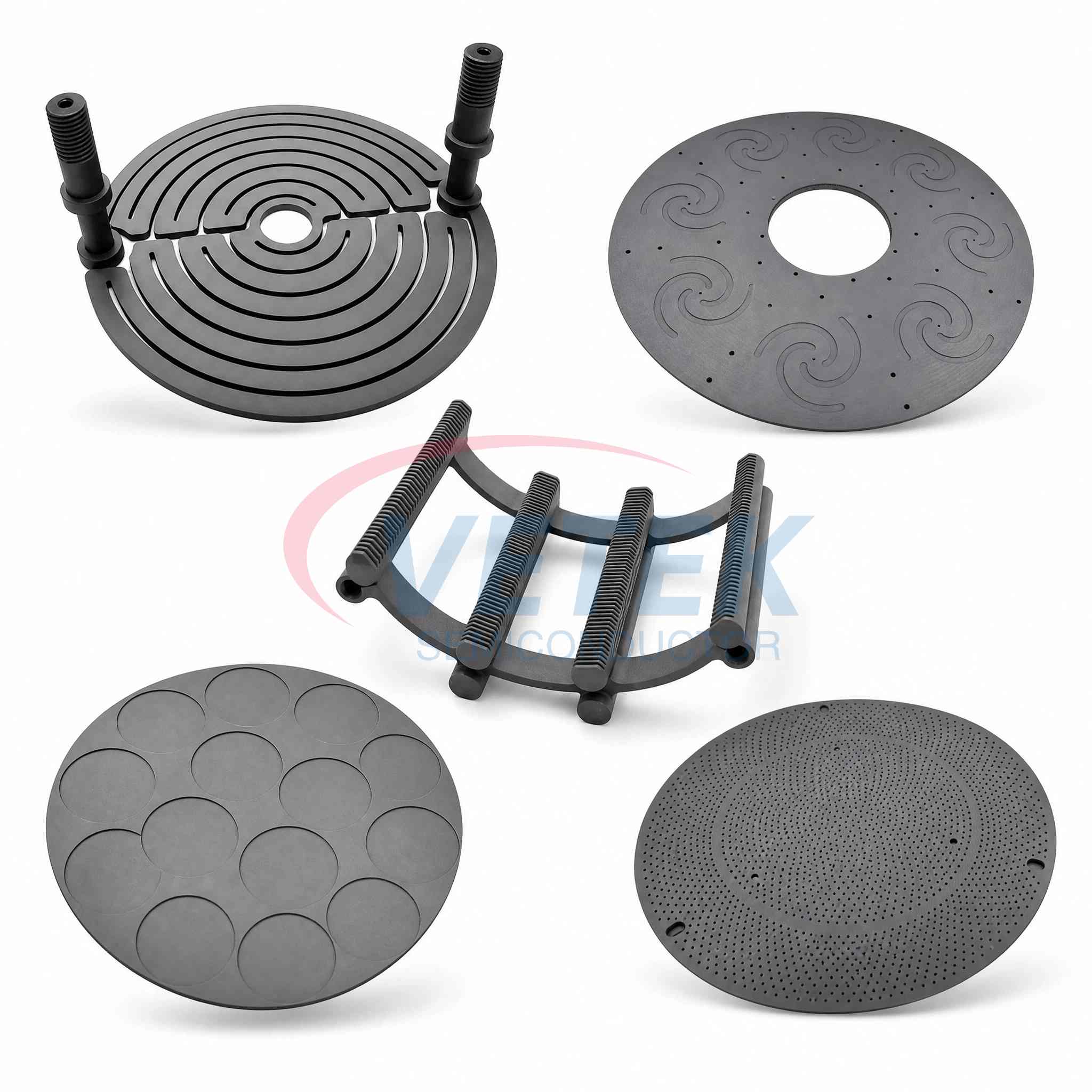
VeTek Semiconductor’s VEECO MOCVD wafer susceptor is a critical component, meticulously engineered using ultrapure graphite with a silicon carbide (SiC) coating. This SiC coating provides numerous benefits, most notably enabling efficient thermal transfer to the substrate. Achieving optimal thermal distribution across the substrate is essential for uniform temperature control, ensuring consistent, high-quality thin-film deposition, which is crucial in semiconductor device fabrication.
Matrix of material properties
Key indicators VeTek standard Traditional solutions
Base material purity 6N isostatic graphite 5N molded graphite
CTE matching degree (25-1400℃) Δα ≤0.3×10⁻⁶/ k Δα ≥1.2×10⁻⁶/K
Thermal conductivity @800℃ 110 W/m·K 85 W/m·K
Surface roughness (Ra) ≤0.1μm ≥0.5μm
Acid tolerance (PH=1@80℃) 1500 cycles 300 cycles
Thermal management innovation
Atomic CTE matching technique
Japan Toyo carbon graphite/SGL substrate + gradient SiC coating
Thermal cycle stress reduced by 82% (measured 1400℃↔RT 500 cycles without cracking)
12-zone temperature compensation structure: achieves ±0.5℃ uniformity on the surface of the φ200mm wafer
Dynamic thermal response: Temperature gradient ≤1.2℃/cm at 5℃/s heating rate
50μm dense SiC main protective layer
Nanotac transition layer (optional)
Gas phase infiltration densification
Verified by ASTM G31-21:
Cl base corrosion rate < 0.003mm/year
NH3 exposed for 1000h without grain boundary corrosion
Digital twin processing
Five-axis machining center: Position accuracy ±1.5μm
Online 3D scanning inspection: 100% full size verification (in accordance with ASME Y14.5)
Third generation semiconductor mass production
Application scenario Process parameters Customer benefits
GaN HEMT 6 inch /150μm epitaxial two-dimensional electron gas density fluctuation < 2%
SiC MOSFET C doping uniformity ±3% threshold voltage deviation is reduced by 40%
Micro LED wavelength uniformity ±1.2nm chip bin rate increased by 15%
Maintenance cost optimization
Cleaning period is extended by 3 times: HF:HNO ₃=1:3 high intensity cleaning is supported
Spare parts life prediction system: AI algorithm accuracy of ±5%
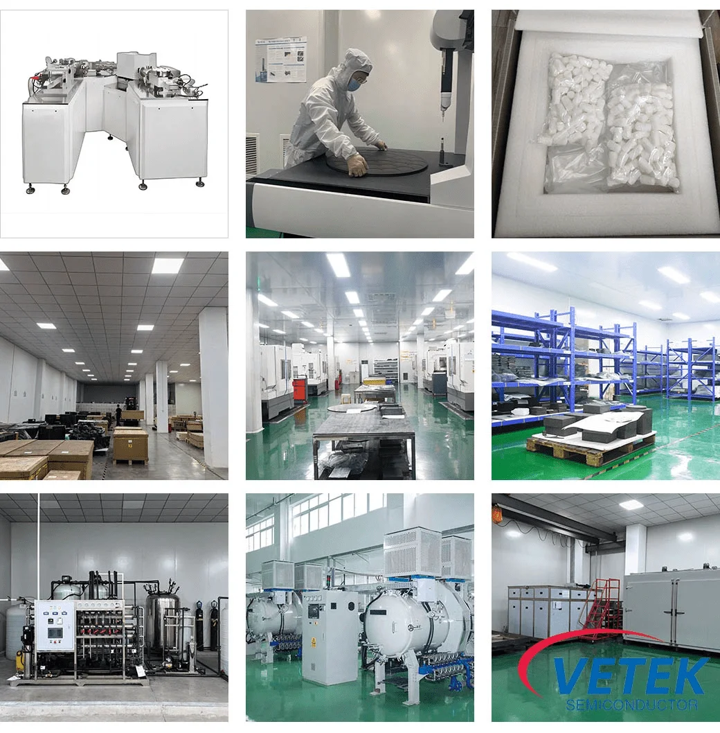
VeTek Semiconductor VEECO MOCVD Susceptor Shops:
Address
Wangda Road, Ziyang Street, Wuyi County, Jinhua City, Zhejiang Province, China
Tel
+86-579-87223657
Wangda Road, Ziyang Street, Wuyi County, Jinhua City, Zhejiang Province, China