Products

China CVD SiC coating wafer Epi susceptor Manufacturer, Supplier, Factory

Assume full accountability to meet all requires of our purchasers; realize continual advancements by selling the advancement of our customers; grow to be the final permanent cooperative partner of consumers and maximize the interests of clientele for CVD SiC coating wafer Epi susceptor, CVD SiC coating, Wafer Epi susceptor, SiC coated Wafer Susceptor, SiC Coating Epi susceptor, Never-ending improvement and striving for 0% deficiency are our two main quality policies. Should you need anything, don't hesitate to contact us.
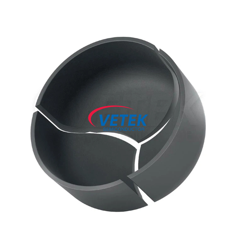
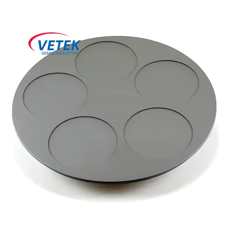
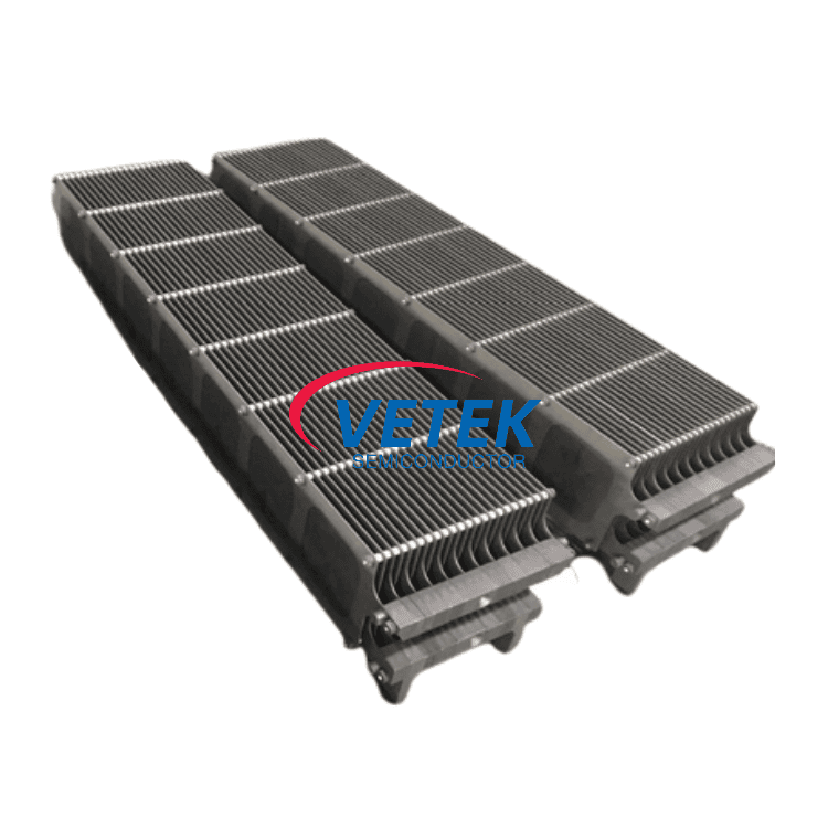
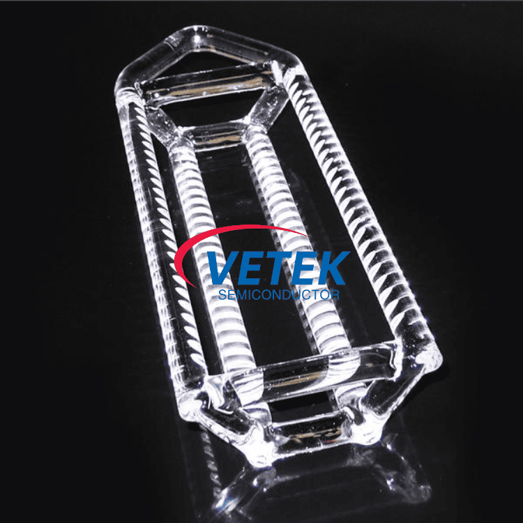
CVD SiC coating wafer Epi susceptor, We give good quality but unbeatable low price and the best service. Welcome to post your samples and color ring to us .We are going to produce the items according to your request. If you are interested in any solutions we provide, remember to feel free to contact us directly by mail, fax, telephone or internet. We have been here to answer your questions from Monday to Saturday and looking forward to cooperating with you.

Hot Products

  • Isostatic Graphite Crucible

    Isostatic Graphite Crucible

    As a leading supplier of customized graphite crucibles in China, VeTek Semiconductor mainly provides Isostatic Graphite Crucible, SiC Coated Graphite Crucible Deflector, Glassy Carbon Coated Graphite Crucible, etc. Our graphite crucibles are made of high-purity graphite raw materials and manufactured through precision technology, with excellent high temperature resistance, corrosion resistance and thermal conductivity. Welcome to consult us.
  • Single wafer epi graphite susceptor

    Single wafer epi graphite susceptor

    Veteksemicon Single wafer epi graphite susceptor is designed for high-performance silicon carbide (SiC), gallium nitride (GaN) and other third generation semiconductor epitaxial process, and is the core bearing component of high-precision epitaxial sheet in mass production.Welcome your further inquiry.
  • Silicon Carbide Coating Wafer Holder

    Silicon Carbide Coating Wafer Holder

    The Silicon Carbide Coating Wafer Holder by Veteksemicon is engineered for precision and performance in advanced semiconductor processes such as MOCVD, LPCVD, and high-temperature annealing. With a uniform CVD SiC coating, this wafer holder ensures exceptional thermal conductivity, chemical inertness, and mechanical strength — essential for contamination-free, high-yield wafer processing.
  • CVD TaC Coating Crucible

    CVD TaC Coating Crucible

    VeTek Semiconductor is a professional manufacturer and leader of CVD TaC Coating Crucible products in China. CVD TaC Coating Crucible is based on tantalum carbon (TaC) coating. The tantalum carbon coating is evenly covered on the surface of the crucible through chemical vapor deposition (CVD) process to enhance its heat resistance and corrosion resistance. It is a material tool specially used in high temperature extreme environments. Welcome your further consultation.
  • Wafer Handling Robotic Arm

    Wafer Handling Robotic Arm

    Vetek Semiconductor thermal spraying technology plays a vital role in the application of wafer handling robotic arms, especially in semiconductor manufacturing environments that require high precision and high cleanliness. This technology significantly improves the durability, reliability and work efficiency of the equipment by coating special materials on the surface of the wafer handling robotic arm. Welcome to inquiry us.
  • Large sized resistance heating SiC crystal growth furnace

    Large sized resistance heating SiC crystal growth furnace

    Silicon carbide crystal growth is a core process in the manufacturing of high-performance semiconductor devices. The stability, precision, and compatibility of crystal growth equipment directly determine the quality and yield of silicon carbide ingots. Based on the characteristics of Physical Vapor Transport (PVT) technology, Veteksemi has developed a resistance heating furnace for silicon carbide crystal growth, enabling stable growth of 6-inch, 8-inch, and 12-inch silicon carbide crystals with full compatibility with conductive, semi-insulating, and N-type material systems. Through precise control of temperature, pressure, and power, it effectively reduces crystal defects such as EPD (Etch Pit Density) and BPD (Basal Plane Dislocation), while featuring low energy consumption and a compact design to meet the high standards of industrial large-scale production.

Send Inquiry

X
We use cookies to offer you a better browsing experience, analyze site traffic and personalize content. By using this site, you agree to our use of cookies. Privacy Policy
Reject Accept