About Us

About Us

WuYi TianYao New Material Tech.Co.,Ltd.
WuYi TianYao New Material Tech.Co.,Ltd., founded in 2016, is a leading provider of advanced coating materials for the semiconductor industry. Our founder, a former expert from the Chinese Academy of Sciences' Institute of Materials, established the company with a focus on developing cutting-edge solutions for the industry.

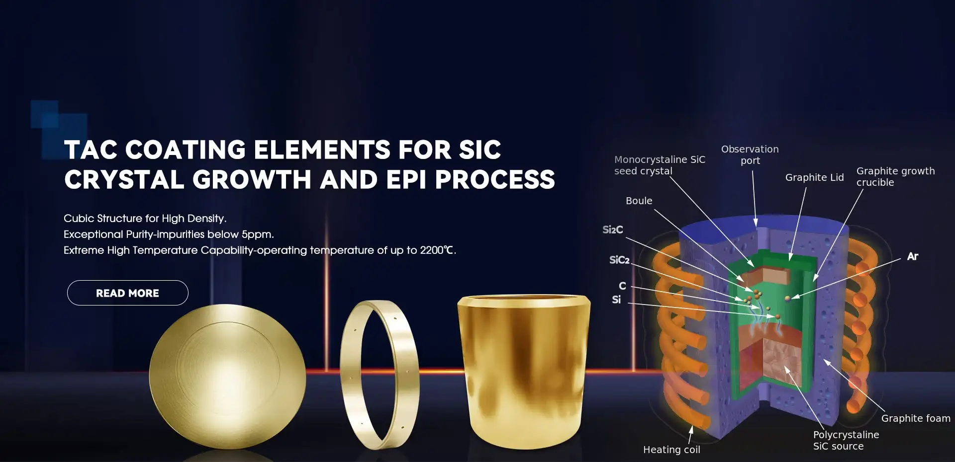
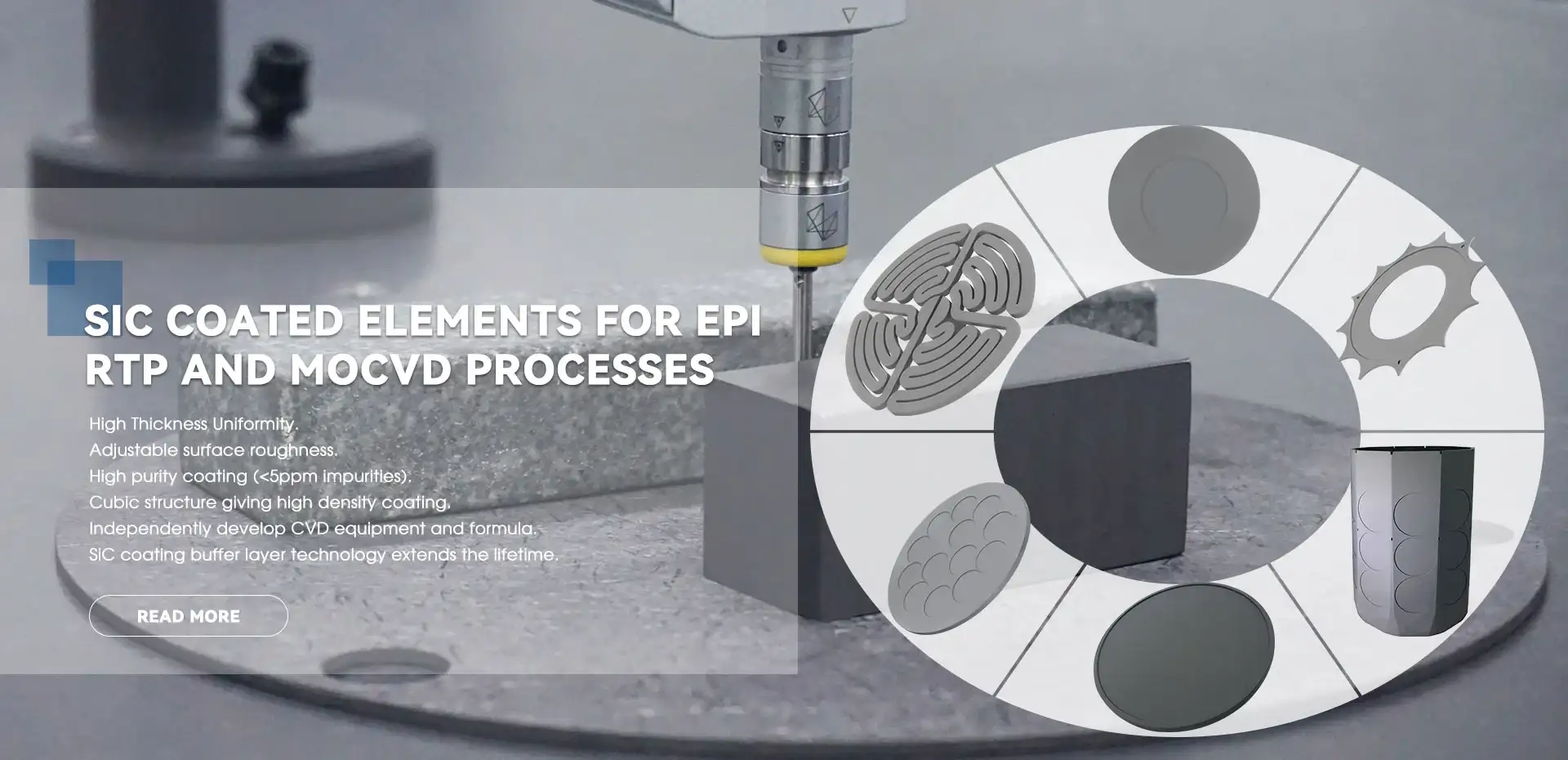
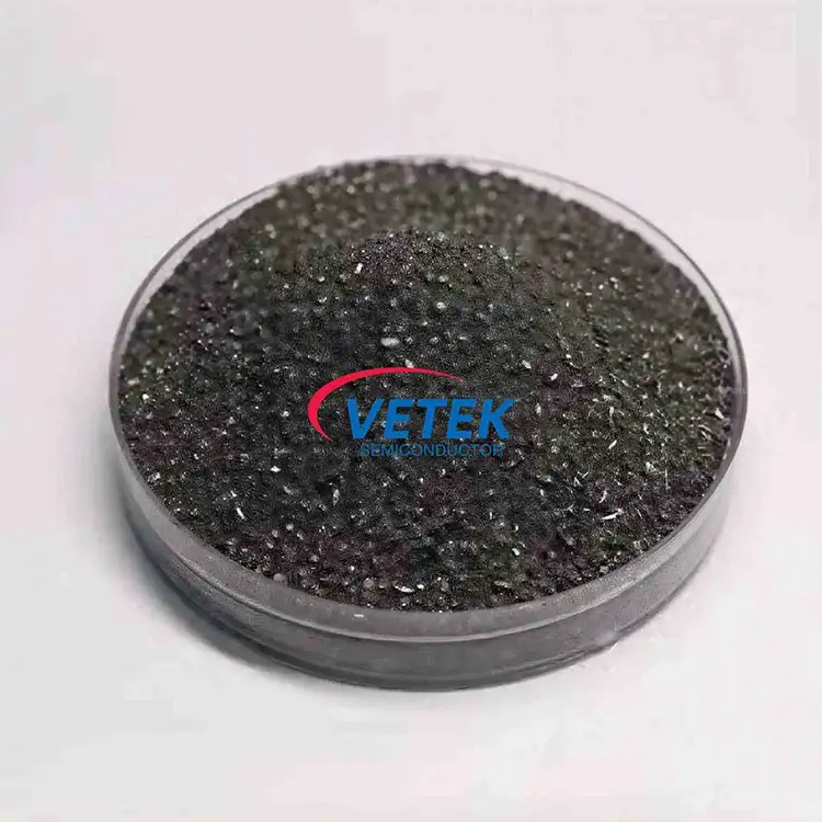
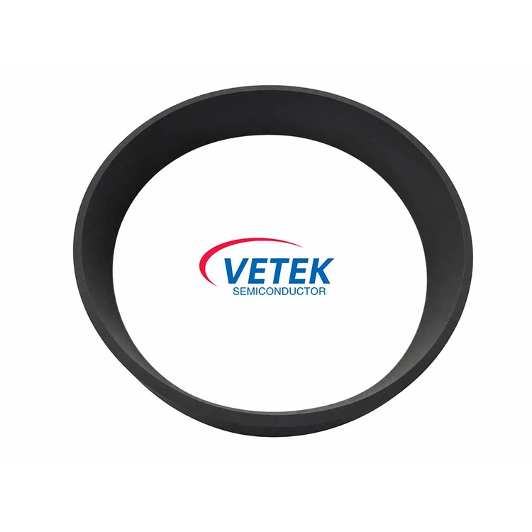
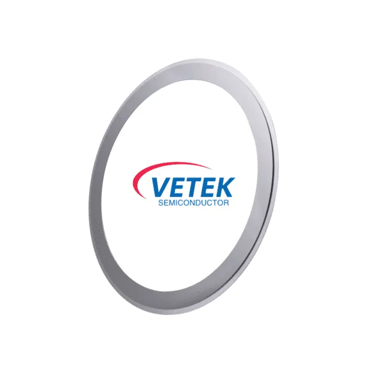
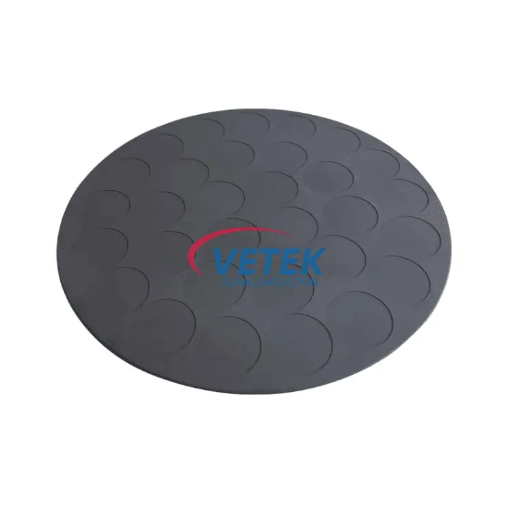
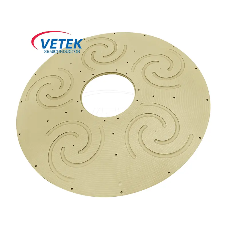
Our main product offerings include CVD silicon carbide (SiC) coatings, tantalum carbide (TaC) coatings, bulk SiC, SiC powders, and high-purity SiC materials. The main products are SiC coated graphite susceptor, preheat rings, TaC coated diversion ring, halfmoon parts, etc., the purity is below 5ppm, can meet customer requirements.

150

Employees

12

Production Lines

2

Production Bases

2

R&D Centers
View More
VeTek is the professional of the Silicon Carbide Coating, Tantalum Carbide Coating, Special Graphite manufacturer and supplier in china. You can rest assured to buy the products from our factory and we will offer you the quality after-sale service.

Our Services

CNC Machining

CNC Machining

Material Sintering

Material Sintering

Material Purification

Material Purification

CVD Coating

CVD Coating

Material Testing

Material Testing

Our advantages

Advanced materials change the future. Aimed to be the leading semiconductor materials innovator worldwide.

Advanced Equipment & Testing Capacity

Advanced Equipment & Testing Capacity

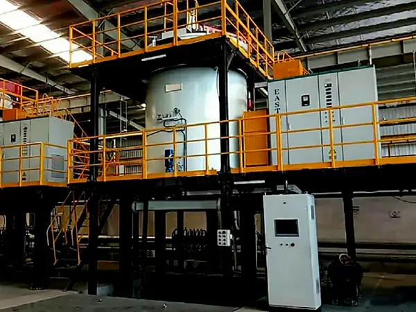
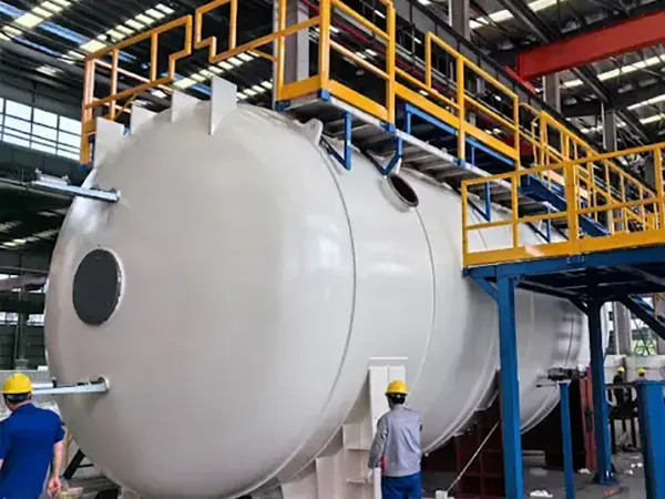
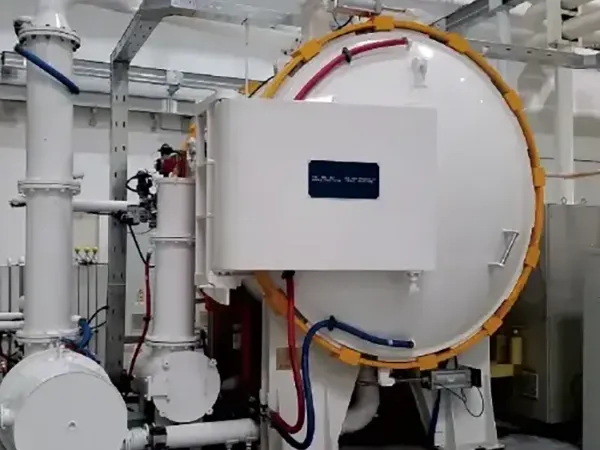
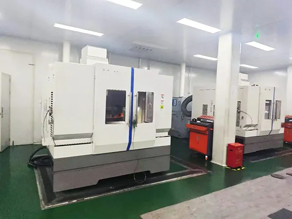
We operate 12 advanced production lines with over 80 sets of industry-leading CVD and inspection equipment to ensure stable mass production and strict quality control.

Dual R&D Centers & Deep Expertise

Dual R&D Centers & Deep Expertise

Founded by a former CAS professor with a 30%+ annual R&D investment, our dual R&D platforms successfully bridge the gap between underlying mechanism research and industrial scale-up.

Strategic Industry Recognition

Strategic Industry Recognition

As a recognized guide enterprise in the integrated circuit industry chain, VeTek Semiconductor has received strategic capital investments from multiple top-tier listed semiconductor leaders.

High-Purity & High-Barrier Solutions

High-Purity & High-Barrier Solutions

We deliver high-purity, temperature-resistant CVD coatings and components that effectively extend service lifespans and optimize production costs for global semiconductor and PV clients.

FACTORY INTRODUCTION

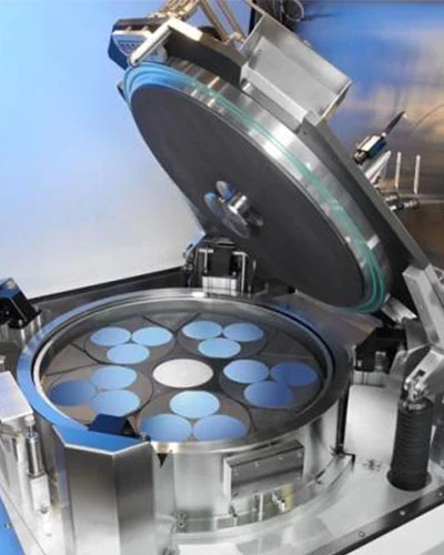
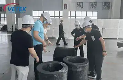
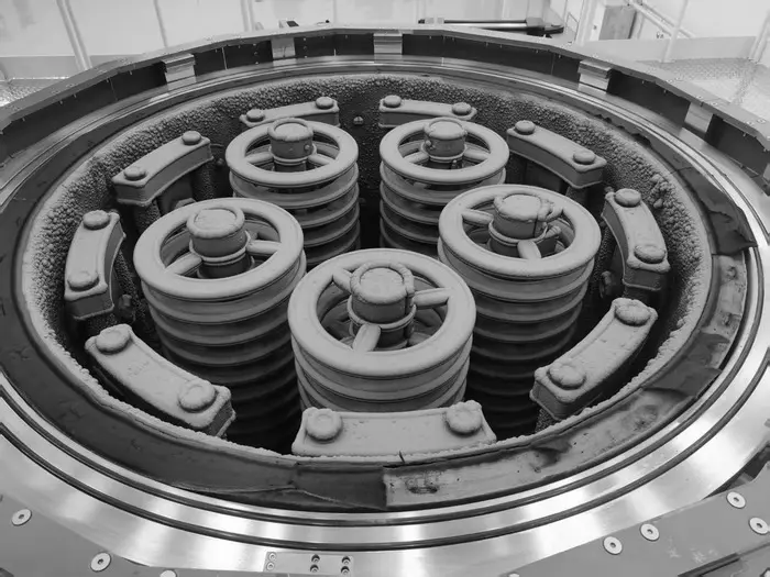
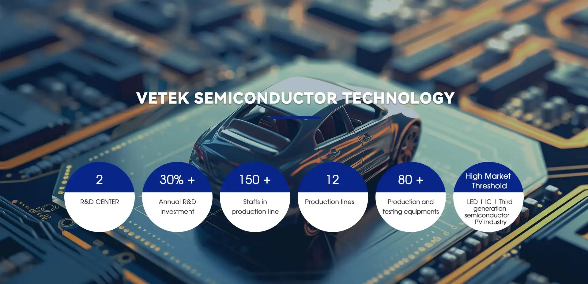
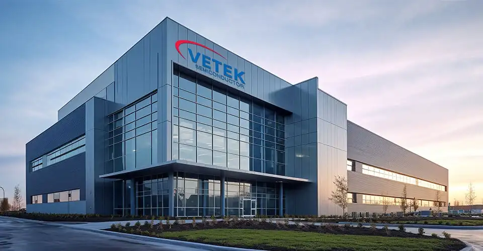
VeTek Semiconductor operates dual research and development centers, integrating R&D and production capabilities. Currently has 2 production bases, 12 production lines, 150+ employees, R & D accounted for more than 30%, our team focuses on technology, production, sales and operation management, and has a strong comprehensive ability. Product layout is mainly used in LED, IC integrated circuit, third generation semiconductor, photovoltaic and other industries.

WHAT OUR CLIENTS SAY

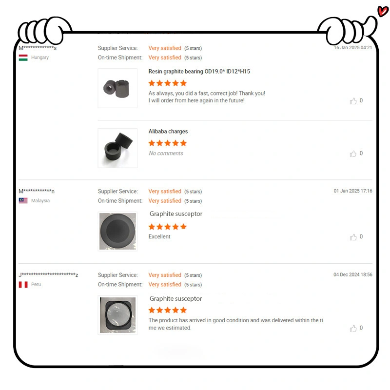
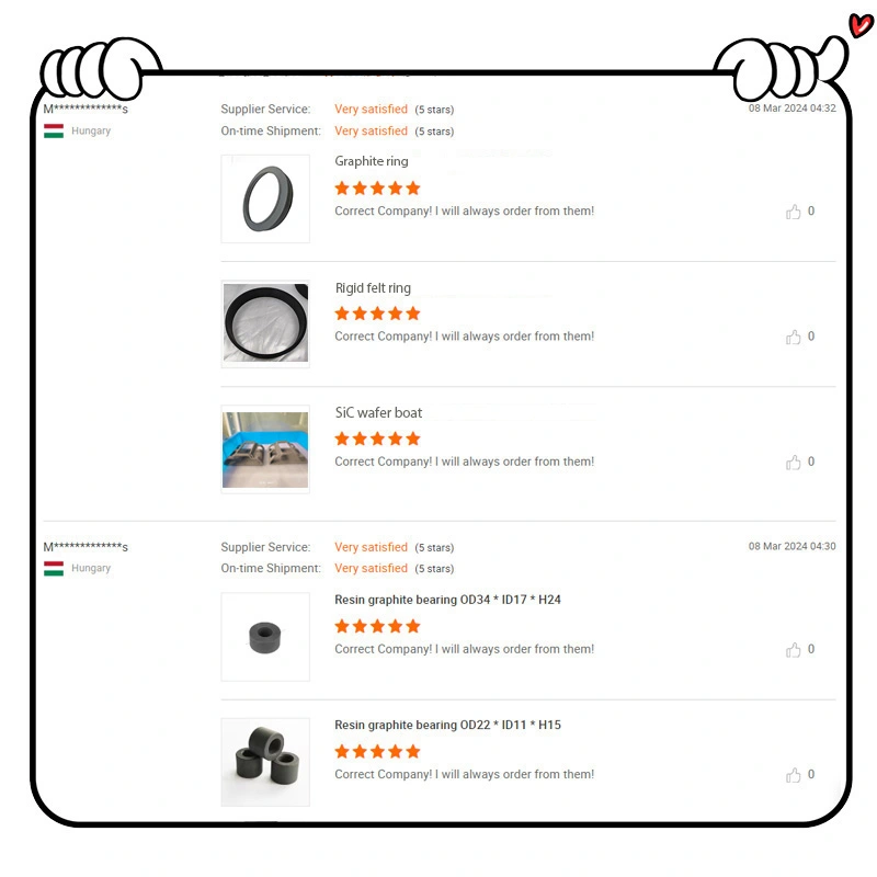
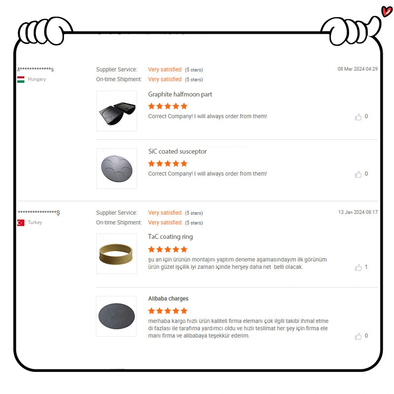
WHAT OUR CLIENTS SAY

APPLICATION FIELD

APPLICATION FIELD
APPLICATION FIELD
APPLICATION FIELD
APPLICATION FIELD

FAQ

Q1: Can your coating products and solid components be fully customized to our blueprints?

A: Yes, absolute customization is our core strength. We provide end-to-end custom machining based on your precise drawings, selecting the most suitable substrates and matching them with high-uniformity CVD SiC or TaC coatings to perfectly fit your semiconductor equipment.

Q2: How do you guarantee the high purity required for semiconductor-grade materials?

A: We implement strict raw material screening and advanced high-temperature purification processes. All elements are trace-analyzed using professional testing equipment like ICP-OES and GDMS to ensure our coatings and graphite components meet the ultra-pure, particle-free standards of the chip industry.

Q3: What quality management system and industry certifications do you have?

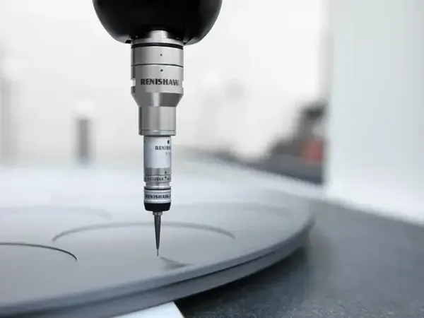
A: Our production facility operates in strict accordance with the ISO9001 quality management system. From substrate machining to the final chemical vapor deposition (CVD) process, every step undergoes rigorous dimensional and surface precision checks before shipment.

Q4: Do you support sample testing before placing bulk orders, and what is the process?

A: Yes, we welcome sample evaluation for custom susceptors, wafer boats, or dummy wafers. You can provide your specific operational parameters or equipment models (such as LPE, Aixtron, or ASM), and we will deliver a trial sample to ensure it meets your thermal and process requirements.

Q5: What is your typical production lead time for standard and custom products?

A: For standard configurations or available inventory, we ship immediately. For custom items requiring precision machining and CVD coating processing, lead times usually range from 3 to 6 weeks, depending on the design complexity and batch volume.

Q6: What kind of after-sales technical support do you provide for international clients?

A: We offer 24/7 online technical consulting to help optimize your thermal fields and component lifespan. If any operational issues or concentration fluctuations occur during process integration, our R&D engineers will work with you remotely to provide quick and practical solutions.

News

X
We use cookies to offer you a better browsing experience, analyze site traffic and personalize content. By using this site, you agree to our use of cookies.Privacy Policy
RejectAccept