Products

China SiC Wafer Manufacturer, Supplier, Factory

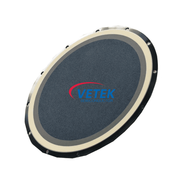
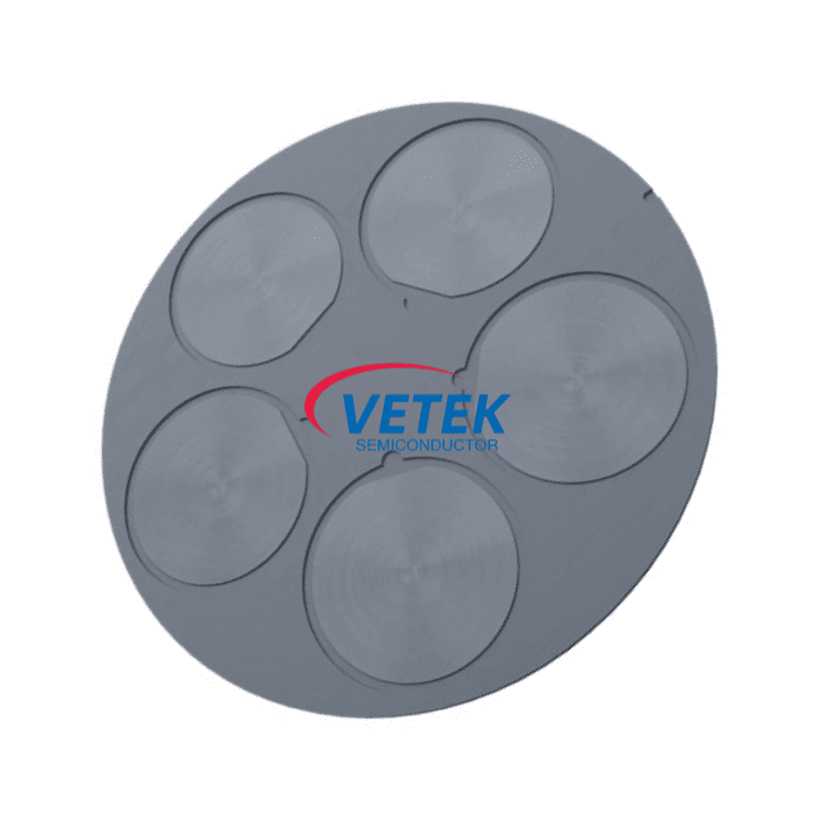
We know that we only thrive if we can guarantee our combined rate competiveness and good quality advantageous at the same time for SiC Wafer, 4H N-type SiC Substrate, 4H SiC Substrate, Silicon carbide Wafer, 2 inch 4off axis p-type SiC Wafer, Many years of work experience, we have realized the importance of providing good quality products and the best before-sales and after-sales services.
SiC Wafer, We care about every steps of our services, from factory selection, product development & design, price negotiation, inspection, shipping to aftermarket. Now we have implemented a strict and complete quality control system, which ensures that each product can meet quality requirements of customers. Besides, all of our solutions have been strictly inspected before shipment. Your Success, Our Glory: Our aim is to help customers realize their goals. We're making great efforts to achieve this win-win situation and sincerely welcome you to join us.

Hot Products

  • Ultra Pure Graphite Lower Halfmoon

    Ultra Pure Graphite Lower Halfmoon

    VeTek Semiconductor is a leading supplier of customized Ultra Pure Graphite Lower Halfmoon in China, specializing in advanced materials for many years. Our Ultra Pure Graphite Lower Halfmoon is specifically designed for SiC epitaxial equipment, ensuring excellent performance. Made from ultra-pure imported graphite, it offers reliability and durability. Visit our factory in China to explore our high-quality Ultra Pure Graphite Lower Halfmoon firsthand.Welcome to consult at any time.
  • High purity quartz boat

    High purity quartz boat

    Our High purity quartz boat is made of fused quartz (SiO₂ content ≥ 99.99%). With its excellent resistance to extreme environments, low thermal expansion coefficient, and long life cycle, it has become an irreplaceable key consumable in the semiconductor and new energy industries.
  • Semiconductor thermal spraying technology

    Semiconductor thermal spraying technology

    Vetek Semiconductor Semiconductor thermal spraying technology is an advanced process that sprays materials in a molten or semi-molten state onto the surface of a substrate to form a coating. This technology is widely used in the field of semiconductor manufacturing, mainly used to create coatings with specific functions on the surface of the substrate, such as conductivity, insulation, corrosion resistance, and oxidation resistance. The main advantages of thermal spraying technology include high efficiency, controllable coating thickness, and good coating adhesion, making it particularly important in the semiconductor manufacturing process that requires high precision and reliability. Looking forward to your inquiry.
  • Solid SiC Gas Shower Head

    Solid SiC Gas Shower Head

    Solid SiC Gas Shower Head plays a major role in making the gas uniform in the CVD process, thereby ensuring uniform heating of the substrate. VeTek Semiconductor has been deeply involved in the field of solid SiC devices for many years and is able to provide customers with customized Solid SiC Gas Shower Heads. No matter what your requirements are, we look forward to your inquiry.
  • SiC coating ALD susceptor

    SiC coating ALD susceptor

    The SiC coating ALD susceptor is a support component specifically used in the atomic layer deposition (ALD) process. It plays a key role in the ALD equipment, ensuring the uniformity and precision of the deposition process. We believe that our ALD Planetary Susceptor products can bring you high-quality product solutions.
  • GaN epitaxial susceptor

    GaN epitaxial susceptor

    As a leading GaN epitaxial susceptor supplier and manufacturer in China, VeTek semiconductor GaN epitaxial susceptor is a high-precision susceptor designed for GaN epitaxial growth process, used to support epitaxial equipment such as CVD and MOCVD. In the manufacturing of GaN devices (such as power electronic devices, RF devices, LEDs, etc.), GaN epitaxial susceptor carries the substrate and achieves high-quality deposition of GaN thin films under high temperature environment. Welcome your further inquiry.

Send Inquiry

X
We use cookies to offer you a better browsing experience, analyze site traffic and personalize content. By using this site, you agree to our use of cookies. Privacy Policy
Reject Accept