Products

China SiC Coating Inlet Ring Manufacturer, Supplier, Factory

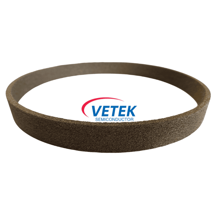
We've been also concentrating on bettering the things management and QC method in order that we could continue to keep terrific benefit inside the fiercely-competitive company for SiC Coating Inlet Ring, CVD SiC coating ring, SiC coating ring, cvd sic coated, SiC coating graphite ring, Welcome all nice buyers communicate specifics of products and ideas with us!!
SiC Coating Inlet Ring, If any item be of curiosity to you, make sure you allow us to know. We will try our best to satisfy your requirements with high quality products and solutions, the best prices and prompt delivery. Be sure to feel free to contact us at any time. We'll reply you when we receive your inquiries. You should note that samples are available before we start our business.

Hot Products

  • Ion Beam Sputter sources grid

    Ion Beam Sputter sources grid

    Ion beam is mainly used for ion etching, ion coating and plasma injection. The role of the Ion Beam Sputter sources grid is to dissect the ions and accelerate them to the required energy. Vetek Semiconductor provides high purity graphite ion beam Ion Beam Sputter sources grid for optical lens ion beam polishing, semiconductor wafer modification, etc. Welcome to inquire about customized products.
  • Silicon Carbide Carrier Plate For LED Etching

    Silicon Carbide Carrier Plate For LED Etching

    Veteksemicon Silicon Carbide Carrier Plate For LED Etching, specifically designed for LED chip manufacturing, is a core consumable in the etching process. Made from precision-sintered high-purity silicon carbide, it offers exceptional chemical resistance and high-temperature dimensional stability, effectively resisting corrosion from strong acids, bases, and plasma. Its low contamination properties ensure high yields for LED epitaxial wafers, while its durability, far exceeding that of traditional materials, helps customers reduce overall operating costs, making it a reliable choice for improving etching process efficiency and consistency.
  • Wafer Handling Robotic Arm

    Wafer Handling Robotic Arm

    Vetek Semiconductor thermal spraying technology plays a vital role in the application of wafer handling robotic arms, especially in semiconductor manufacturing environments that require high precision and high cleanliness. This technology significantly improves the durability, reliability and work efficiency of the equipment by coating special materials on the surface of the wafer handling robotic arm. Welcome to inquiry us.
  • SiC Coated Graphite Crucible Deflector

    SiC Coated Graphite Crucible Deflector

    The SiC coated graphite crucible deflector is a key component in the single crystal furnace equipment, its task is to guide the molten material from the crucible to the crystal growth zone smoothly, and ensure the quality and shape of the single crystal growth.Vetek semiconductor can provide both graphite and SiC coating material.Welcome to contact us for more details.
  • Silicon Carbide Ceramic Wafer Boat

    Silicon Carbide Ceramic Wafer Boat

    VeTek Semiconductor specializes in providing high-quality wafer boats, pedestals and custom wafer carriers in vertical/column and horizontal configurations to meet various semiconductor process requirements. As a leading manufacturer and supplier of silicon carbide coating films, our silicon carbide ceramic wafer boat is favored by the European and American markets for their high cost-effectiveness and excellent quality, and are widely used in advanced semiconductor manufacturing processes. VeTek Semiconductor is committed to establishing long-term and stable cooperative relationships with global customers, and especially hopes to become your reliable semiconductor process partner in China.
  • Silicon carbide Cantilever Paddle for Wafer Processing

    Silicon carbide Cantilever Paddle for Wafer Processing

    The Silicon Carbide Cantilever Paddle from Veteksemicon is engineered for advanced wafer processing in semiconductor manufacturing. Made of high-purity SiC, it delivers outstanding thermal stability, superior mechanical strength, and excellent resistance to high temperatures and corrosive environments. These features ensure precise wafer handling, extended service life, and reliable performance in processes such as MOCVD, epitaxy, and diffusion. Welcome to consult.

Send Inquiry

X
We use cookies to offer you a better browsing experience, analyze site traffic and personalize content. By using this site, you agree to our use of cookies. Privacy Policy
Reject Accept