Products

China CVD TaC Coating Ring Manufacturer, Supplier, Factory

Our commission is to serve our buyers and purchasers with most effective good quality and aggressive portable digital goods for CVD TaC Coating Ring, CVD TAC Coating, TAC Coating, TaC Guide Ring, CVD TaC coating cover, Our experienced specialized group will be wholeheartedly at your support. We sincerely welcome you to check out our site and enterprise and send out us your inquiry.
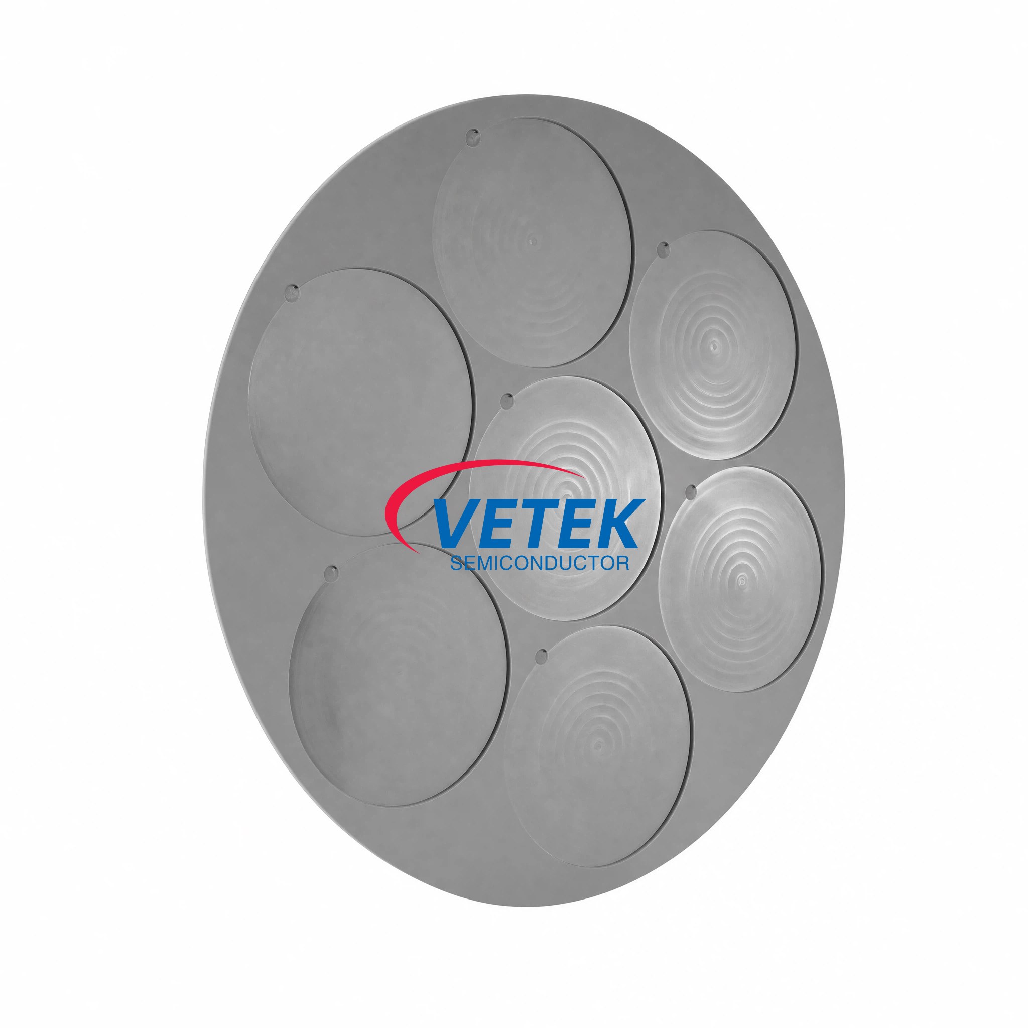
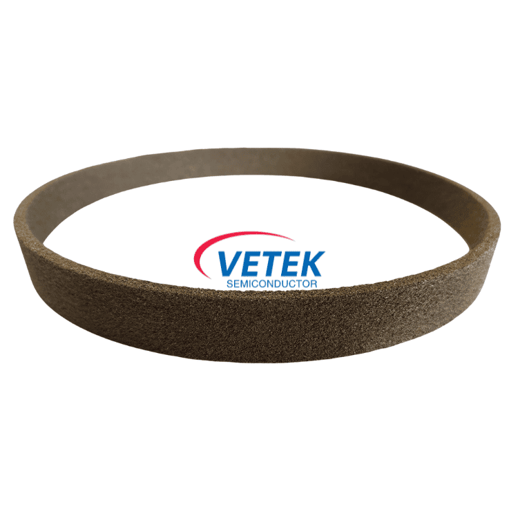
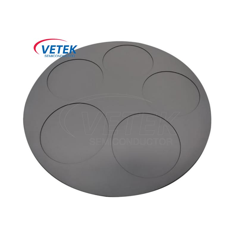
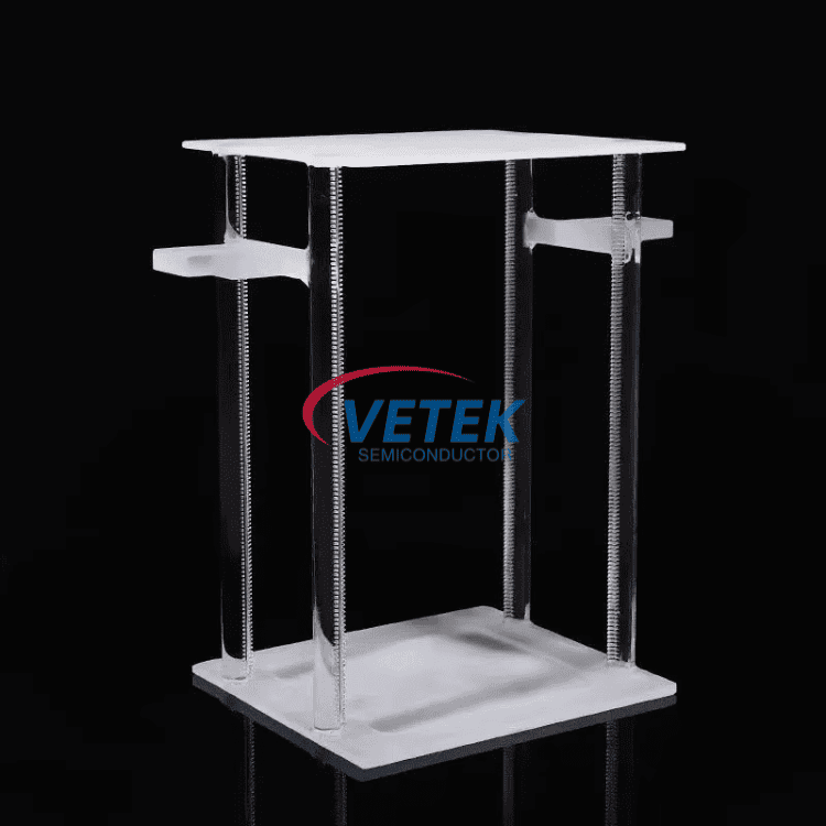
CVD TaC Coating Ring, We've got been perfectly devoted to the design, R&D, manufacture, sale and service of hair products during 10 years of development. We now have introduced and are making full use of internationally advanced technology and equipment, with advantages of skilled workers. "Dedicated to providing reliable customer service" is our aim. We've been sincerely looking forward to establishing business relationships with friends from at home and abroad.

Hot Products

  • Tantalum Carbide Coating Ring

    Tantalum Carbide Coating Ring

    VeTek semiconductor Tantalum Carbide Coating Ring is a indispensable component in the semiconductor industry, specifically in the etching of SiC wafers. Its combination of a graphite base and TaC coating ensures superior performance in high-temperature and chemically aggressive environments. With its enhanced thermal stability, corrosion resistance, and mechanical strength, the Tantalum Carbide Coated Ring helps semiconductor manufacturers achieve precision, reliability, and high-quality results in their production processes.
  • Quartz Wafer Boats

    Quartz Wafer Boats

    Our Quartz Wafer Boats are high-purity wafer carrier solution tailored for semiconductor, LED, solar cell, and battery manufacturing processes. Engineered to endure high temperatures and chemically aggressive environments, this quartz boat features low thermal expansion, excellent electrical insulation, and long-term dimensional stability. Ideal for diffusion, oxidation, and LPCVD processes, it supports precise wafer alignment and is available in various sizes to meet different equipment requirements.
  • SiC Crystal Growth New Technology

    SiC Crystal Growth New Technology

    Vetek Semiconductor's ultra-high purity silicon carbide (SiC) formed by chemical vapor deposition (CVD) is recommanded to be used as a source material for growing silicon carbide crystals by physical vapor transport (PVT). In SiC Crystal Growth New Technology, the source material is loaded into a crucible and sublimated onto a seed crystal. Use the high purity CVD-SiC blocks to be as a source for growing SiC crystals. Welcome to establish a partnership with us.
  • Tantalum Carbide Coated Tube for Crystal Growth

    Tantalum Carbide Coated Tube for Crystal Growth

    Tantalum Carbide Coated Tube for Crystal Growth is mainly used in SiC crystal growth process. VeTek Semiconductor has been supplying Tantalum Carbide Coated Tube for Crystal Growth for many years and has been working in the field of TaC coating for many years. Our products have a high purity and high temperature resistance. We look forward to becoming your long-term partner in China. Feel free to inquire us.
  • SiC Coated Support Ring

    SiC Coated Support Ring

    VeTek Semiconductor is a professional China manufacturer and supplier, mainly producing SiC coated support rings, CVD silicon carbide (SiC) coatings, tantalum carbide (TaC) coatings. We are committed to providing perfect technical support and ultimate product solutions for the semiconductor industry, welcome to contact us.
  • Porous SiC Ceramic Chucks

    Porous SiC Ceramic Chucks

    The Porous SiC Ceramic Chuck by Veteksemicon is a precision-engineered vacuum platform designed for secure and particle-free wafer handling in advanced semiconductor processes such as etching, ion implantation, CMP, and inspection. Manufactured from high-purity porous silicon carbide, it offers outstanding thermal conductivity, chemical resistance, and mechanical strength. With customizable pore sizes and dimensions, Veteksemicon delivers tailored solutions to meet the stringent demands of cleanroom wafer processing environments.

Send Inquiry

X
We use cookies to offer you a better browsing experience, analyze site traffic and personalize content. By using this site, you agree to our use of cookies. Privacy Policy
Reject Accept